Difference between revisions of "Projects:2015s1-28 Wireless Rotation Detector"
(→Antenna Design) |
(→1.Method) |
||
| (32 intermediate revisions by the same user not shown) | |||
| Line 69: | Line 69: | ||
can strongly respond to a properly oriented electric field due to the capacitor-like structure | can strongly respond to a properly oriented electric field due to the capacitor-like structure | ||
when the circuit is driven by EM field at resonant frequency. | when the circuit is driven by EM field at resonant frequency. | ||
| − | [[File: Example of Metamaterial Absorber and equivalent.png|400px|thumb|center| | + | |
| + | [[File: Example of Metamaterial Absorber and equivalent.png|400px|thumb|center|Figure 1.Example of Metamaterial Absorber and equivalent]] | ||
The metamaterial absorber is expected to have the ability of dissipating the incident waves inside of the structure with limited energy reflected back from it [8]. As shown in Figure 2, the incident wave is transmitted into the substrate at working frequency. The surface current will be created along the ground plane when the wave reached the bottom layer. Similarly, remaining energy will be reflected back to the resonators which will also generate another surface current on the top layer. These two currents have same magnitude with opposite directions, resulting in a destructive interference [8]. Hence, the thickness of the substrate should be carefully chosen for the effective destructive interference. | The metamaterial absorber is expected to have the ability of dissipating the incident waves inside of the structure with limited energy reflected back from it [8]. As shown in Figure 2, the incident wave is transmitted into the substrate at working frequency. The surface current will be created along the ground plane when the wave reached the bottom layer. Similarly, remaining energy will be reflected back to the resonators which will also generate another surface current on the top layer. These two currents have same magnitude with opposite directions, resulting in a destructive interference [8]. Hence, the thickness of the substrate should be carefully chosen for the effective destructive interference. | ||
| − | [[File: Metamaterial Absorption Structure.png|400px|thumb|center| | + | |
| + | [[File: Metamaterial Absorption Structure.png|400px|thumb|center|Figure 2.Metamaterial Absorption Structure]] | ||
== Key Requirements == | == Key Requirements == | ||
| Line 126: | Line 128: | ||
== Schedule and Milestone == | == Schedule and Milestone == | ||
*Milestone in Semester 1 | *Milestone in Semester 1 | ||
| − | [[File:Milestone in Semester 1.png|400px|thumb|center| | + | [[File:Milestone in Semester 1.png|400px|thumb|center|Table 1.Milestone in Semester ]] |
*Milestone in Semester 2 | *Milestone in Semester 2 | ||
| − | [[File:Milestone in Semester 2.png|400px|thumb|center| | + | [[File:Milestone in Semester 2.png|400px|thumb|center|Table 2.Milestone in Semester 2]] |
== Metamaterial Absorber Design == | == Metamaterial Absorber Design == | ||
| − | 1. Method | + | === 1.Method === |
| − | 1.1 Metamaterial Absorber Design | + | '''''1.1 Metamaterial Absorber Design''''' |
According to the introduction given in the Section 1.3, the existing absorber can only absorb 36% of incident power at 2.4 GHz when it has the same polarization with the antenna. The main cause for this is that the bandwidth of the existing metamaterial absorber is only 0.03 GHz, which is too narrow. As a consequence, the performance of the absorber will significantly drop if the resonant frequency slightly shifts. Accordingly, the main purpose for the new absorber design is to achieve distinct absorption performance and relatively wide bandwidth. | According to the introduction given in the Section 1.3, the existing absorber can only absorb 36% of incident power at 2.4 GHz when it has the same polarization with the antenna. The main cause for this is that the bandwidth of the existing metamaterial absorber is only 0.03 GHz, which is too narrow. As a consequence, the performance of the absorber will significantly drop if the resonant frequency slightly shifts. Accordingly, the main purpose for the new absorber design is to achieve distinct absorption performance and relatively wide bandwidth. | ||
| Line 141: | Line 143: | ||
| − | 1.1.1 Structure Tapering | + | '''''1.1.1 Structure Tapering''''' |
| Line 158: | Line 160: | ||
In order to reduce the Q factor and remain the same resonant frequency, we tapered the loop width to increase the inductance and increased the gap to decrease the capacitance of the ELC resonator. Figure 4 compares the original ELC resonator and the tapered one. The original structure we proposed has an ELC resonator and a ground plane, separated by the FR4 substrate with height of 3.2mm. The ELC resonator has the dimensions of a=15mm, g=0.4mm, d=12.6mm, b=0.8mm, l=3.6mm and copper thickness of t=0.035mm. The tapered resonator has the gap size varied from 0.4mm to 2.0mm and loop width decreased from 0.8mm to 0.1mm. | In order to reduce the Q factor and remain the same resonant frequency, we tapered the loop width to increase the inductance and increased the gap to decrease the capacitance of the ELC resonator. Figure 4 compares the original ELC resonator and the tapered one. The original structure we proposed has an ELC resonator and a ground plane, separated by the FR4 substrate with height of 3.2mm. The ELC resonator has the dimensions of a=15mm, g=0.4mm, d=12.6mm, b=0.8mm, l=3.6mm and copper thickness of t=0.035mm. The tapered resonator has the gap size varied from 0.4mm to 2.0mm and loop width decreased from 0.8mm to 0.1mm. | ||
| − | [[File:ELC_resonator_and_tapered_one.PNG|400px|thumb|center| | + | [[File:ELC_resonator_and_tapered_one.PNG|400px|thumb|center|Figure 3.ELC_resonator_and_tapered_one]] |
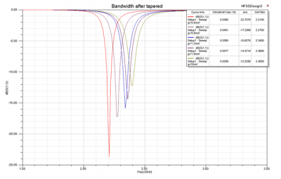
From Figure 5 illustrates the reflection coefficient S11 for the metamaterial absorber. The transmission coefficient is 0 because of the metal ground plane. It is interesting to note that the metamaterial absorber resonates at frequency of 2.4GHz with minimum reflection coefficient -18.75dB with the bandwidth is 0.0389GHz. | From Figure 5 illustrates the reflection coefficient S11 for the metamaterial absorber. The transmission coefficient is 0 because of the metal ground plane. It is interesting to note that the metamaterial absorber resonates at frequency of 2.4GHz with minimum reflection coefficient -18.75dB with the bandwidth is 0.0389GHz. | ||
| − | [[File:Reflection coefficient for the metamaterial absorber.PNG|400px|thumb|center|figure 5.Reflection coefficient for the metamaterial absorber|thumb| | + | [[File:Reflection coefficient for the metamaterial absorber.PNG|400px|thumb|center|figure 5.Reflection coefficient for the metamaterial absorber|thumb|Figure 4.Reflection coefficient for the metamaterial absorber]] |
| − | [[File:Reflection coefficients for tapered MMA.PNG|400px|thumb|center| | + | [[File:Reflection coefficients for tapered MMA.PNG|400px|thumb|center|Figure 5.Reflection coefficients for tapered MMA]] |
| − | Figure | + | Figure 5 shows the changes in the bandwidth as the gap size increases from 0.4 to 2mm. We can conclude that the bandwidth increases as gap size g increases until 0.8mm, then the bandwidth keeps decreasing as gap size increases, which is completely different from the analysis about Q factor before. In addition, we can observe that the return loss at resonance also increases as the gap size increases. |
| − | The reason for the results mentioned above can be explained by using interference theory, which leads to the multiple reflection and transmission inside of the absorber structure. Figure | + | The reason for the results mentioned above can be explained by using interference theory, which leads to the multiple reflection and transmission inside of the absorber structure. Figure 2 shows that the metamaterial absorber has 2 layers: resonator and ground plane. The overall reflection is the superposition of the multiple transmissions and reflections [12], which is defined as: |
[[File:Formula 1.PNG|400px|thumb|center|]] | [[File:Formula 1.PNG|400px|thumb|center|]] | ||
| Line 176: | Line 178: | ||
The formula demonstrates that the overall reflection is associated with the reflection and transmission coefficient of ELC resonator, the reflection coefficient of ground plane, the height of the substrate and the angle of incidence. Hence, the overall bandwidth of the reflection coefficient may be too small if we substitute all relevant values into the formula. Also, due to the complexity of the overall reflection, the bandwidth enhancement by structure tapering may not work for the metamaterial absorber since we only increased the bandwidth of the ELC resonator. | The formula demonstrates that the overall reflection is associated with the reflection and transmission coefficient of ELC resonator, the reflection coefficient of ground plane, the height of the substrate and the angle of incidence. Hence, the overall bandwidth of the reflection coefficient may be too small if we substitute all relevant values into the formula. Also, due to the complexity of the overall reflection, the bandwidth enhancement by structure tapering may not work for the metamaterial absorber since we only increased the bandwidth of the ELC resonator. | ||
| − | 1.1.2 Substrate Height | + | '''''1.1.2 Substrate Height''''' |
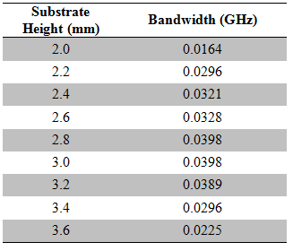
We then investigated the impacts of the substrate height on the absorptivity and bandwidth. Based on the structure proposed in Section 4.1.1, we varied the substrate height from 2mm to 3.6mm. | We then investigated the impacts of the substrate height on the absorptivity and bandwidth. Based on the structure proposed in Section 4.1.1, we varied the substrate height from 2mm to 3.6mm. | ||
| − | [[File:Table 1.PNG|400px|thumb|center|Table | + | [[File:Table 1.PNG|400px|thumb|center|Table 3. Bandwidth for different substrate height]] |
| − | Table | + | Table 3 shows the bandwidth as the substrate height changes. It is interesting to note that the bandwidth starts with 0.0164 at 2.4GHz and increases until height increases to 2.8mm. Then the bandwidth start to decrease as the substrate height keeps increases. The optimized result we can obtain was 0.0398GHz, which is still relatively narrow. |
The reason for this can still be explained by the formula in section 4.11. Due to the complexity of the overall reflection, the bandwidth cannot be significantly improved by only changing the substitute height. In conclusion, the bandwidth still does not meet the specification although it can be slightly increased by varying the substrate height. | The reason for this can still be explained by the formula in section 4.11. Due to the complexity of the overall reflection, the bandwidth cannot be significantly improved by only changing the substitute height. In conclusion, the bandwidth still does not meet the specification although it can be slightly increased by varying the substrate height. | ||
| − | 1.1.3 Via | + | '''''1.1.3 Via''''' |
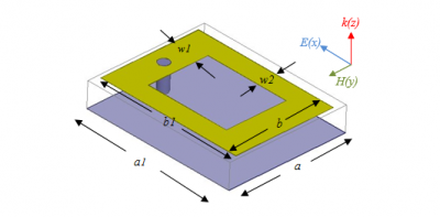
After some unsuccessful trials, we finally presented the design of the metamaterial absorber operating at 2.4 GHz by using a via. A unit cell of proposed absorber is shown in Figure 7. It is a 3 layer structure which has a metallic loop at the top, a ground plane and a substrate in between. A 150Ω resistive load is used as a via to connect the top and bottom layer. The absorber is designed to operate at 2.4 GHz with the optimized dimensions given by a1=20mm, a=16mm, b1=19mm, b=13.4mm, w1=4, w2=2.6mm. | After some unsuccessful trials, we finally presented the design of the metamaterial absorber operating at 2.4 GHz by using a via. A unit cell of proposed absorber is shown in Figure 7. It is a 3 layer structure which has a metallic loop at the top, a ground plane and a substrate in between. A 150Ω resistive load is used as a via to connect the top and bottom layer. The absorber is designed to operate at 2.4 GHz with the optimized dimensions given by a1=20mm, a=16mm, b1=19mm, b=13.4mm, w1=4, w2=2.6mm. | ||
| − | [[File:A schematic showing the proposed unit cell of metamaterial absorber.PNG|400px|thumb|center| | + | [[File:A schematic showing the proposed unit cell of metamaterial absorber.PNG|400px|thumb|center|Figure 6a.A schematic showing the proposed unit cell of metamaterial absorber]] |
| + | |||
| + | [[File:Prototype of absorber design.PNG|400px|thumb|center|Figure 6b.Prototype of absorber design]] | ||
The unit cell was hosted on the top of a 3.2mm thick FR-4 dielectric substrate with a loss tangent of 0.025 and a dielectric constant of εr=4.4. The simulation for ELC resonator was performed with a full-wave electromagnetic simulator, Ansoft HFSS. The unit cell was placed in a waveguide with Master and Slave boundary condition. The boundary condition was selected for the unit cell in order to realize TEM mode excitation with polarization shown in Figure 7. | The unit cell was hosted on the top of a 3.2mm thick FR-4 dielectric substrate with a loss tangent of 0.025 and a dielectric constant of εr=4.4. The simulation for ELC resonator was performed with a full-wave electromagnetic simulator, Ansoft HFSS. The unit cell was placed in a waveguide with Master and Slave boundary condition. The boundary condition was selected for the unit cell in order to realize TEM mode excitation with polarization shown in Figure 7. | ||
| − | [[File:Reflection coefficient for the metamaterial absorber.PNG|400px|thumb|center| | + | [[File:Reflection coefficient for the metamaterial absorber.PNG|400px|thumb|center|Figure 7.Reflection coefficient for the metamaterial absorber]] |
| − | Figure | + | Figure 7 illustrates the performance of the absorber for both co-polarized direction and cross-polarized direction. From the graph, it is obvious that the absorber resonates at 2.4 GHz with reflection coefficient S11 of -26.3 dB for the co-polarization direction. In the meanwhile, the reflection coefficient for cross-polarization is 0 dB at 2.4 GHz. Using scattering parameters, the absorptivity is calculated by A=1-|S11|^2-〖|S21|〗^2, where S21 is 0 due to the ground plane. Therefore, the absorption rate is 99.77% based on the simulation results. |
In addition, it is interesting to note that the bandwidth of the metamaterial absorber has been significantly increased to 0.2 GHz, which is 7 times more than that of the original design. | In addition, it is interesting to note that the bandwidth of the metamaterial absorber has been significantly increased to 0.2 GHz, which is 7 times more than that of the original design. | ||
| − | [[File:Surface current distribution for co-polarization.PNG|400px|thumb|center| | + | [[File:Surface current distribution for co-polarization.PNG|400px|thumb|center|Figure 8.Surface current distribution for co-polarization]] |
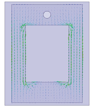
| − | The reason why the design can successfully absorb power can be analysed by the surface current distribution, as shown in Figure | + | The reason why the design can successfully absorb power can be analysed by the surface current distribution, as shown in Figure 8. From the graph, we can observe that the surface current is mainly distributed at the middle of the left and right side of metallic loop. Meanwhile, the surface current at the top and bottom is minimal. |
However, the voltage at the surface will be distributed conversely. The voltage at top and bottom of the metallic loop is maximum while that at middle of left and right side is minimum. Therefore, connecting the top layer and ground plane with a resistive load enables the current to flow through the resistor due to the voltage difference, resulting in the power dissipation. | However, the voltage at the surface will be distributed conversely. The voltage at top and bottom of the metallic loop is maximum while that at middle of left and right side is minimum. Therefore, connecting the top layer and ground plane with a resistive load enables the current to flow through the resistor due to the voltage difference, resulting in the power dissipation. | ||
| + | |||
| + | === 2.Experiment & Result === | ||
| + | |||
| + | '''''2.1 Absorber Test''''' | ||
| + | |||
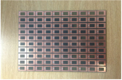
| + | Based on the simulated unit cell structure, a 10×10 metamaterial absorber array has been fabricated, as shown in Appendix B. The unit cells were hosted on the FR4 substrate with height of 3.2mm. The copper thickness for top and bottom layers is 0.035mm. | ||
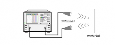
| + | The experiment was conducted in the Anechoic Chamber in order to mitigate the interference from the environment. Figure 11 demonstrates how the experiment was conducted in the Anechoic Chamber. To measure the absorption capability of the absorber, a pair of horn antennas, severing as transmitter and receiver of the power, was placed separately by the distance of 40 cm and connected to the Agilent N5230A analyser with low loss cables. | ||
| + | |||
| + | |||
| + | [[File:A schematic for absorber experiment.PNG|400px|thumb|center|Figure 9.A schematic for absorber experiment]] | ||
| + | |||
| + | |||
| + | The absorber was placed in middle front of the 2 antennas. In order to ensure the accuracy of the measurement, the distance between the absorber and the antennas was 140 cm to avoid the near-field effects. However, the transmitting and receiving antennas would have incident angle of 8.13º with respect to the surface of the absorber plane due to the experiment limitations. | ||
| + | |||
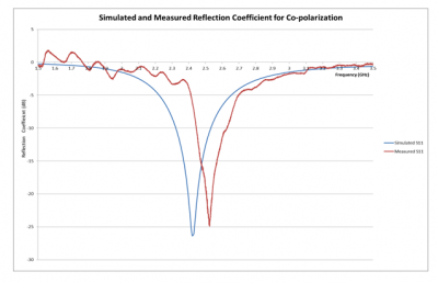
| + | Firstly, we measured the power reflected by a copper sheet which has the same size as the absorber. Then, we tested reflection response by substituting the absorber for the copper sheet. The difference between two power responses can be considered as the absorption rate of the metamaterial absorber. The measured results are shown below: | ||
| + | |||
| + | [[File:Simulated and measured reflection coefficient for co-polarization.PNG|400px|thumb|center|Figure 10.Simulated and measured reflection coefficient for co-polarization ]] | ||
| + | |||
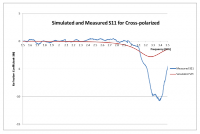
| + | [[File:Simulated and measured reflection coefficient for cross-polarization.PNG|400px|thumb|center|Figure 11.Simulated and measured reflection coefficient for cross-polarization ]] | ||
| + | |||
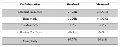
| + | [[File:Summary for simulation and measurment for co-polarization.PNG|400px|thumb|center|Table 4.Summary for simulation and measurment for co-polarization ]] | ||
| + | |||
| + | Table 4 summarises the simulated and experimental results for the absorber at co-polarized direction. It is obvious that bandwidth, reflection coefficient and absorptivity for both are similar to each other. However, it is interesting to note that the resonant frequency for the measurement is 2.52 GHz, which is different from the simulated one. | ||
| + | |||
| + | Figure 11 shows the reflection coefficient for the cross-polarized direction. We can observe that the reflection coefficient for both simulation and measurement is 0 at 2.4 GHz, which means the absorber can reflect 100% incident power when cross-polarized. In addition, both results show that the resonant frequency at around 3.25 GHz. The difference between simulated and measured minimum reflect coefficients may result from the unwanted edge scattering caused by the finite array of unit cell | ||
| + | |||
| + | === Discussion === | ||
| + | |||
| + | From the results related to the absorber, we can conclude that the simulated results are very close to the measured ones except for the resonant frequency. The simulated resonant frequency is 2.4 GHz while the measured one is actually 2.52 GHz. This section will include a detailed discussion on the discrepancy between 2 resonant frequencies. | ||
| + | The final design uses a 150 ohm resistor as a via to connect the top and bottom layer. In the fabrication process, the resistor we used is called MMA 0204, which is one of the professional thin film MELF resistors. | ||
| + | |||
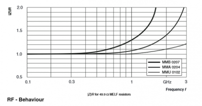
| + | [[File:RF behaviour of MMA 0204.PNG|400px|thumb|center|Figure 12.RF behaviour of MMA 0204 ]] | ||
| + | |||
| + | The RF behaviour of the MMA 0204 is illustrated in Figure 12. It is clear that MMA 0204 is purely resistive until 0.6 GHz. After that, the ratio of the total impedance to the resistance significantly increases beyond 1, which means the resistor will have capacitance or inductance at high frequency. | ||
| + | From the graph, we can find that |Z|/R is roughly 1.7 at frequency of 2.4 GHz. Hence, the total impedance Z of the resistor at 2.4 GHz is given by: | ||
| + | |||
| + | Z=R(1+1.375j), where R is 150Ω | ||
| + | |||
| + | Accordingly, we need to consider the RF behaviour of MMA 0204 at 2.4 GHz in new simulation to obtain more accurate results. | ||
| + | |||
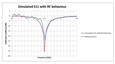
| + | [[File:Simulated S11 with RF behaviour of the resistor.PNG|400px|thumb|center|Figure 13.Simulated S11 with RF behaviour of the resistor ]] | ||
| + | |||
| + | |||
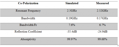
| + | [[File:Summary for simulation and measurement.PNG|400px|thumb|center|Table 5.Summary for simulation and measurement ]] | ||
| + | |||
| + | Figure 13 shows the simulated S11 with RF behaviour considered and all results are summarised in Table 5. We can clearly see that resonant frequencies for the simulation and measurement are very close to each other, which means the resistor could be the potential reason which causes the resonant frequency shift. | ||
== Antenna Design == | == Antenna Design == | ||
| − | + | === 1.Method === | |
| + | |||
| − | |||
This section is related to antenna design method and will introduce two failed methods and a successful method that is able to reduce the coupling between two antennas less than -40dB. The absorber design method and software algorithm will be introduced in latter section. | This section is related to antenna design method and will introduce two failed methods and a successful method that is able to reduce the coupling between two antennas less than -40dB. The absorber design method and software algorithm will be introduced in latter section. | ||
| − | 1.1 Antenna structure design method | + | '''''1.1 Antenna structure design method''''' |
According to the project requirement, transmission and receiving antennas should be on same side. So the dual patch antennas are decided for this project. The dual patch antennas should be built on same substrate and one is used to receiving and another one is used to transmission. So the antennas structure should be designed at first. The dimensions of the microstrip path antenna are determined by following parameters: | According to the project requirement, transmission and receiving antennas should be on same side. So the dual patch antennas are decided for this project. The dual patch antennas should be built on same substrate and one is used to receiving and another one is used to transmission. So the antennas structure should be designed at first. The dimensions of the microstrip path antenna are determined by following parameters: | ||
| Line 230: | Line 280: | ||
* The length of rectangle (y0) which should be substrate on patch | * The length of rectangle (y0) which should be substrate on patch | ||
| − | 1.2 Reducing coupling method | + | '''''1.2 Reducing coupling method''''' |
Using the ‘U’ shape structure between two patch antennas. | Using the ‘U’ shape structure between two patch antennas. | ||
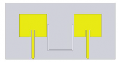
From figure 6, this method is also cutting slots on ground plane between two same directional patch antennas and the ‘U’ shape is composed of three slots. The principle of the ‘U’ shape structure is based on an isolation of reverse phase coupling for reducing coupling. | From figure 6, this method is also cutting slots on ground plane between two same directional patch antennas and the ‘U’ shape is composed of three slots. The principle of the ‘U’ shape structure is based on an isolation of reverse phase coupling for reducing coupling. | ||
| − | [[File:Dual patch antennas with 'U' structure.PNG|400px|thumb|center| | + | [[File:Dual patch antennas with 'U' structure.PNG|400px|thumb|center|Figure 14.Dual patch antennas with 'U' structure]] |
| − | 2. Antenna results | + | === 2. Antenna results === |
| − | 2.1 Design calculation result: | + | '''''2.1 Design calculation result:''''' |
As referred above, in order to increase the bandwidth of antenna, the RT/duroid 5880 has been chosen as substrate. The substrate parameters and the desired resonance frequency of the antenna are as follow: | As referred above, in order to increase the bandwidth of antenna, the RT/duroid 5880 has been chosen as substrate. The substrate parameters and the desired resonance frequency of the antenna are as follow: | ||
| Line 254: | Line 304: | ||
* The length of rectangle (y0) which should be substrate on patch | * The length of rectangle (y0) which should be substrate on patch | ||
| − | [[File:Calculated parameters of patch antenna.PNG|400px|thumb|center| | + | [[File:Calculated parameters of patch antenna.PNG|400px|thumb|center|Table 6.Calculated parameters of patch antenna]] |
| − | [[File:Optimal result for parameters.PNG|400px|thumb|center| | + | [[File:Optimal result for parameters.PNG|400px|thumb|center|Table 7.Optimal result for parameters]] |
| − | 2.2 Simulated and measured result | + | '''''2.2 Simulated and measured result''''' |
This section includes single antenna, dual patch antennas without ‘U’ structure, and dual patch antennas with ‘U’ structure. Each situation contains simulated result, measured result and comparison as well as relevant discussion. | This section includes single antenna, dual patch antennas without ‘U’ structure, and dual patch antennas with ‘U’ structure. Each situation contains simulated result, measured result and comparison as well as relevant discussion. | ||
| Line 265: | Line 315: | ||
* Single patch antenna: | * Single patch antenna: | ||
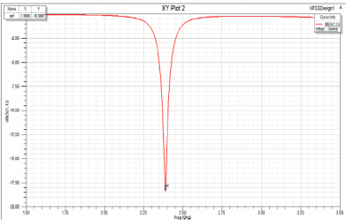
| − | The Figure | + | The Figure below illustrates the reflection coefficient at resonate frequency 2.4GHz. The S11 is around -23.78dB at resonance frequency 2.4GHz, which means nearly 99.3% energy has been transmitted through the patch antenna. The reflection coefficient is lower and the input impedance match the transmission line. So the input impedance is close to 50 ohms. |
| − | [[File:Reflection coefficient for single patch antenna.PNG|400px|thumb|center| | + | [[File:Reflection coefficient for single patch antenna.PNG|400px|thumb|center|Figure 15.Reflection coefficient for single patch antenna ]] |
* Dual patch antennas (Without ‘U’ structure): | * Dual patch antennas (Without ‘U’ structure): | ||
| Line 274: | Line 324: | ||
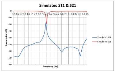
The following figures illustrate simulated results of reflection coefficient S11 and coupling effect S21 of dual patch antenna without ‘U’ structure. | The following figures illustrate simulated results of reflection coefficient S11 and coupling effect S21 of dual patch antenna without ‘U’ structure. | ||
| − | Simulated result: | + | '''Simulated result:''' |
| − | |||
| − | |||
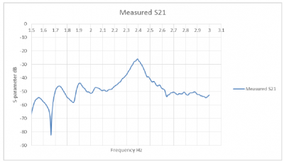
| + | [[File:Reflection coefficient & coupling effect for dual patch antennas.PNG|400px|thumb|center|Figure 16.Reflection coefficient & coupling effect for dual patch antennas]] | ||
| − | Measured results: | + | '''Measured results:''' |
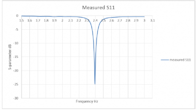
The following figures illustrate measured results of reflection coefficient S11 and coupling effect S21 for dual patch antennas. | The following figures illustrate measured results of reflection coefficient S11 and coupling effect S21 for dual patch antennas. | ||
| − | [[File:Measured reflection coefficient for dual patch antennas.PNG|400px|thumb|center| | + | [[File:Measured reflection coefficient for dual patch antennas.PNG|400px|thumb|center|Figure 17.Measured reflection coefficient for dual patch antennas]] |
| − | [[File:Measured coupling effect for dual patch antennas.PNG|400px|thumb|center| | + | [[File:Measured coupling effect for dual patch antennas.PNG|400px|thumb|center|Figure 18.Measured coupling effect for dual patch antennas ]] |
| − | Comparison: | + | ''Comparison:'' |
From figures above, comparing simulated result of reflection coefficient S11 that is around -19dB at resonance frequency 2.4GHz with measured result of reflection coefficient S11 that is -18dB at 2.4GHz, it is obviously that the simulated result is very close to measure results and the resonate frequency is in ISM frequency bandwidth. The S11 result is acceptable. | From figures above, comparing simulated result of reflection coefficient S11 that is around -19dB at resonance frequency 2.4GHz with measured result of reflection coefficient S11 that is -18dB at 2.4GHz, it is obviously that the simulated result is very close to measure results and the resonate frequency is in ISM frequency bandwidth. The S11 result is acceptable. | ||
| Line 296: | Line 345: | ||
* Dual patch antennas with ‘U’ structure: | * Dual patch antennas with ‘U’ structure: | ||
Using ‘U’ structure between two antennas, the following figures illustrate simulated result of reflection coefficient and coupling effect as well as measured. | Using ‘U’ structure between two antennas, the following figures illustrate simulated result of reflection coefficient and coupling effect as well as measured. | ||
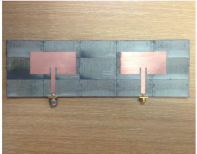
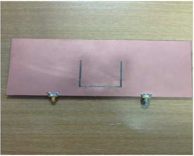
| − | The figure | + | The figure 20 and figure 21 illustrate prototype of dual patch antennas with ‘U’ structure |
| + | |||
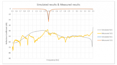
| + | [[File:Simulated results with measured results.PNG|400px|thumb|center|Figure 19.Simulated results with measured results]] | ||
| + | |||
| + | [[File:Top view of dual antennas.png|400px|thumb|center|Figure 20.Top view of dual antennas]] | ||
| + | |||
| + | [[File:Bottom view of dual antennas.png|400px|thumb|center|Figure 21.Bottom view of dual antennas]] | ||
| + | |||
| + | ''Comparison:'' | ||
| + | |||
| + | From figure 19, after using ‘U’ structure between two patch antennas, the reflection coefficient of simulated is around -19dB at resonate frequency 2.4GHz and measured reflection coefficient is around -24dB at 2.4GHz. Those two results are similar with each other and the performance is acceptable. | ||
| + | For the crosstalk efficient, the crosstalk efficient of simulated at resonate frequency is around -43.3dB and the measured crosstalk efficient is -45dB at 2.4GHz. Those two result are close to each other and it is obviously that the coupling between two patch antennas has been reduced dramatically compared with the without ‘U’ structure case. Also from the figure 15, the simulated curve of reflection coefficient overlap the measured one and crosstalk curve of simulated and measured are also similar with each one. The performance of dual patch antennas has met the requirement. The details of principle of ‘U’ will be discussed in next section. | ||
| + | |||
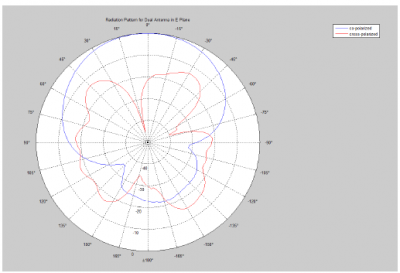
| + | [[File:Radiation Pattern for dual antennas in E-plane.PNG|400px|thumb|center|Figure 22.Radiation Pattern for dual antennas in E-plane]] | ||
| + | |||
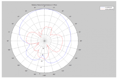
| + | [[File:Radiation Pattern for dual antennas in H-plane.PNG|400px|thumb|center|Figure 23.Radiation Pattern for dual antennas in H-plane]] | ||
| + | |||
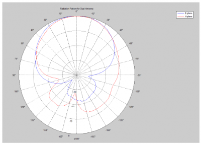
| + | [[File:Radiation Pattern for dual antennas.PNG|400px|thumb|center|Figure 24.Radiation Pattern for dual antennas]] | ||
| + | |||
| + | |||
| + | From figure 22 to figure 24, they demonstrate measured radiation pattern for two patch antennas with ‘U’ structure. All the radiation patterns were measured in the echoic chamber. The two patch antennas system was measured from -180 degree to 180 degree and the measured frequency at 2.4GHz with 1601 sweep points. From the figure 23, it is obviously that the maximum gain in E-plane and H-plane are at 0 degree. So the performance is acceptable and this design has satisfied with the requirement of the project. | ||
| + | |||
| + | ''Results summary:'' | ||
| + | |||
| + | '''Single patch antenna:''' | ||
| + | |||
| + | [[File:Simulated and measured result for single patch antenna.PNG|400px|thumb|center|Table 8.Simulated and measured result for single patch antenna]] | ||
| + | |||
| + | '''Dual patch antennas without ‘U’ structure:''' | ||
| + | |||
| + | |||
| + | [[File:Simulated and measured results for dual patch antennas without 'U'.PNG|400px|thumb|center|Table 9.Simulated and measured results for dual patch antennas without 'U']] | ||
| + | |||
| + | '''Dual patch antennas with ‘U’ structure:''' | ||
| + | |||
| + | [[File:Simulated and measured results for dual patch antennas with 'U'.PNG|400px|thumb|center|Table 10.Simulated and measured results for dual patch antennas with 'U']] | ||
| + | |||
| + | |||
| + | '''''Discussion:''''' | ||
| + | |||
| + | This section will focus on some physical explanations about the ‘U’ structure and explain the reason why the ‘U’ structure can reduce the coupling between two patch antennas. | ||
| + | |||
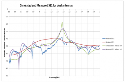
| + | [[File:Simulated and Measured S21 for dual antennas in different conditions.PNG|400px|thumb|center|Figure 25.File:Simulated and Measured S21 for dual antennas in different conditions]] | ||
| + | |||
| + | [[File:Schematic for ‘U’ structure.PNG|400px|thumb|center|Figure 26.Schematic for ‘U’ structure]] | ||
| + | |||
| + | |||
| + | The most important target for this project is reducing the crosstalk between two patch antennas and keeping the antenna system in same plane. Comparing the dual antennas system with ‘U’ structure with antenna system without cut, the figure 25 clearly demonstrates that the coupling between two patch antennas has been reduced nearly 20dB at resonate frequency 2.4GHz no matter what simulation or measurement. The final measured result of coupling is around -45dB which is satisfied with requirement of project. | ||
| + | Actually there are a little bit errors between simulated S21 without ‘U’ structure and measured S21 without ‘U’ structure. The reason is the actual patch antennas system without ‘U’ structure was not fabricated. In order to realize this case, the project group stuck some copper slots to cover ‘U’ structure. So glue could a factor which can affect the measured results. However the errors are in a reasonable range so it is still acceptable. | ||
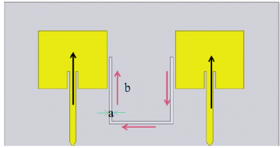
| + | As the figure 26 shows, the letter ‘a’ and ‘b’ represent height and width of a slot. Currently the best size of slot can be obtained through HFSS when a is equal to 46mm and b is equal to 2mm. | ||
| + | The principle of ‘U’ structure is based on an isolation technology of reverse phase coupling. Assuming the signal comes into left patch antenna. From the figure 25, the black arrow indicates the surface current direction in left antenna. Due to the interference between two antennas, this surface current in left antenna would effect on right one and cause a same direction surface current in right patch antenna. However if there is a ‘U’ structure between patch antennas, from the figure 25 the red arrows indicate the surface current flow direction in slots. It is clearly to see the current flowing in right arm is opposite direction compared with original surface current. This opposite direction surface current would cancel out the original coupling in right antenna. So that is the reason why the ‘U’ structure can be used to reduce coupling for strongly coupled antennas. | ||
| + | |||
| + | == Software Design == | ||
| + | The software design consists of 2 main parts. One is the calculation algorithm, which is responsible for calculating the rotation speed. The other one is the user interface, which is used to display the measured data to users. | ||
| + | The main principle used for the calculation algorithm is Fast Fourier Transform (FFT). According to the discussion in Section 1.2, the reflected power shall periodically vary from 0 to maximum due to the polarization loss. Therefore, FFT transforms the received power in time-domain to frequency-domain and the fundamental frequency of the frequency-domain signal provides the information of the rotation speed. The calculation algorithm is reused from the previous design. | ||
| + | |||
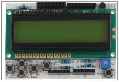
| + | [[File:16×2 LCD keypad shield for Arduino.PNG|400px|thumb|center|Figure 27.16×2 LCD keypad shield for Arduino]] | ||
| + | |||
| + | By contrast, the user interface is adapted this year to display different information. A 16×2 bit LCD keypad is connected to the Arduino UNO board. From Figure 27, it is interesting to note that there are 6 buttons available in the LCD keypad shield. However, only Left, Top, Bottom and Right are used for the message display. | ||
| + | |||
| + | The functionality of the user interface is listed as follows: | ||
| + | |||
| + | *The Greeting Message will be displayed on the screen at the beginning. The message begins with “Hi, Welcome” and “Group 28 Wireless Rotation Detector”, which shifts from right to left on the screen, then the students’ and supervisors’ information shows up. | ||
| + | * The display message can be skipped if “Left” button is pressed. The user interface will then display the rotation speed of objects if the greeting message display is skipped or ends. | ||
| + | * Pressing “Down” button at speed display enables user to read the information regarding power level. The LCD display will show the maximum and minimum power at the screen in dBm. | ||
| + | * Pressing “Up” button at Power display will make software display the rotation speed again. | ||
| + | * The “Right” is used to restart the software system. | ||
| + | |||
| + | == Entire System Test == | ||
| + | |||
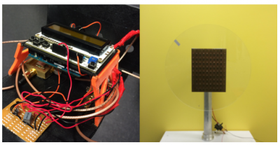
| + | The system test was performed after the absorber and antenna test have been completed. Figure 23 shows the experiment for the system test. We attached the absorber on the centre of a wheel driven by the DC power supply. The dual antennas were hosted at the front part of the housing while the remaining components were mounted on the base. | ||
| + | |||
| + | |||
| + | [[File:Pictures showing the system test.PNG|400px|thumb|center|Figure 23.Pictures showing the system test]] | ||
| + | |||
| + | |||
| + | The purpose of the system test is to test the performance of the entire system from 2 aspects including accuracy and operating distance. | ||
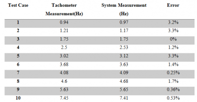
| + | In order to measure the accuracy of the system, a tachometer has been used as a reference. We randomly picked 10 cases which had different rotation speeds, then we measured the speed by using the tachometer and the system we constructed. Finally, we compared the difference between 2 measurements to determine if the system was accurate enough. | ||
| + | For the operational distance test, we made the wheel spin at a fixed speed, then we gradually moved the antennas away from the absorber until “No Connection” was displayed on the screen. Meanwhile, the distance between the antenna and absorber could be considered as the maximum operational distance. | ||
| + | |||
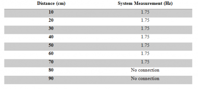
| + | [[File:Measured results from tachometer and constructed system.PNG|400px|thumb|center|Table 11.Measured results from tachometer and constructed system]] | ||
| + | |||
| + | [[File:Operating distance for the constructed system.PNG|400px|thumb|center|Table 12.Operating distance for the constructed system]] | ||
| + | |||
| + | Table 11 shows the results measured by the tachometer and the constructed system. It is clear that the results are very close to each other with the maximum error only 3.3%, which means the system has satisfied the requirement of accuracy. | ||
| + | |||
| + | Table 12 provides the information about the operational distance. From the table, it can be concluded that the maximum distance for the system is roughly 70 cm. Given that the operating distance for the original system was 57 cm [2], the system has already been improved from the respective of the operating distance. | ||
| + | |||
| + | |||
| + | == Conclusion == | ||
| + | |||
| + | The thesis provides the information about the introduction, system design, experiment and result analysis of the wireless rotation detector project. The main objective of this year project is to enhance the performance of the absorber and modify the structure of antenna. | ||
| + | For the absorber design, the metamaterial absorber has the resonant frequency at 2.52 GHz with 99.68% absorptivity. The bandwidth of the absorber is 0.17 GHz, which has been significantly enhanced compared to the simulated result (0.03 GHz) from last year. The potential cause for the resonant frequency shift is also discussed in section 6.1, so current structure of the absorber can be modified with the consideration of resistors’ RF behaviour in order to achieve 2.4 GHz resonant frequency. Overall, the absorber design has successfully met the specifications we proposed at the beginning of the project. | ||
| + | |||
| + | On the part of antenna design, the performance of dual patch antennas is acceptable for our project. The reflection coefficient of dual patch antennas is around a low value at resonate frequency and ensure more than 90% power can be transmitted. The challenge for antenna design is keeping the antenna system in a plane and reducing the coupling less than -40dB. So the isolation technology of a reverse phase coupling has been introduced. So this technology has reduced the coupling between two patch antennas less than -40dB, which can ensure that the transmitting signal would not affect the reading. | ||
| − | + | The requirements about the accuracy and the operating distance of the entire system have also been reached. The entire system can measure the rotation speed within 4% error compared to the commercial product, Tachometer. In addition, the operating distance is also increased from 57 cm to 70 cm under test environment. | |
| + | Overall, the objectives of the project have been achieved and the entire system could be useful for future industrial applications. | ||
== Reference == | == Reference == | ||
Latest revision as of 11:29, 23 October 2015
Contents
Supervisors
Honours students
- 2015: Guowei Deng and Shuopeng Wang
Project objects
Scope
- Design and construct a portable wireless device which can accurately measure the speed of rotating object.
Specific Aims
The aim of the project is to design and construct a portable wireless device which can be used for rotation speed measurement. The device is supposed to consist of antennas, absorbers, Arduino UNO Board with software, etc. The outcomes of the project will be as follows:
- A metamaterial absorber with resonant frequency of 2.4GHz
- A planar dual-antennas with capability of transmitting and receiving signals
- A software system for rotation speed calculation
The device should be able to measure the rotational speed of various objects such as sport equipment, car tyres, turbines, fans, etc. The system shall be operational under a set of circumstances and able to achieve reliable results.
Background & Significance
- Motivation
The rotation speed measurement devices have already ubiquitously used in industries. They are embedded on turbines, wheels or fans to extract the rotation speed of objects. However, most of commonly used angular speed measurement devices, such as laser tachometer, use visible light. One of the constraints in such devices is that the line of sight cannot be impaired [1]. Hence, the optical devices cannot be used if there is an obstacle between rotating objects and the test devices or under sophisticated circumstances such as fog or smoke.
In order to improve the performance of the measurement device, the 2.4GHz electromagnetic waves will be used instead of visible light due to its good ability of propagation. Accordingly, the devices can be used under more complicated situations, even if the line of sight has been impaired, once delivered.
- Technical Background
1. Polarization of Antennas
The polarization of antenna is defined as “the polarization of the wave transmitted (radiated) by the antenna” [2]. There are 3 different types of polarization including linear polarization, circular polarization and elliptical polarization [2]. All of them are defined as “time-varying direction and magnitude of the electric field vector” [2].
2. Polarization Loss Factor
Polarization loss is defined as the power loss due to polarization mismatch. For example, if a horizontally polarized antenna communicates with a vertically polarized antenna, the vertically polarized antenna will transmit vertically polarized waves, while the horizontally polarized antenna can only receive horizontally polarized wave. Thus, there is no power transfer between a horizontally polarized antenna and vertically antenna according to the reciprocity principle. In contrast, if 2 vertically polarized antennas communicate with each other, the power transfer will be maximum. Hence, if two linearly polarized antennas are rotated from each other by an angle θ, the polarization loss factor base on power loss for polarization mismatch is defined as
𝑃𝐿𝐹 = 𝑐𝑜𝑠2θ
3. Metamaterial Absorber
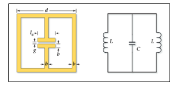
Metamaterials are man-made materials with the unique characteristics, such as negative permittivity and permeability, which cannot be found in natural materials [3]. The metamaterial absorber has been one of the most important applications due to its astonishing properties [4]. A single metallic metamaterial absorber typically consists of a LC resonant circuit and a ground plane, separated by a substrate in between [5]. For example, as shown in Figure 1, the capacitor-like structure can provide capacitance and is connected with two loops in parallel, which can be considered as two inductors in the resonant circuit [6]. The resonator can strongly respond to a properly oriented electric field due to the capacitor-like structure when the circuit is driven by EM field at resonant frequency.
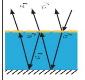
The metamaterial absorber is expected to have the ability of dissipating the incident waves inside of the structure with limited energy reflected back from it [8]. As shown in Figure 2, the incident wave is transmitted into the substrate at working frequency. The surface current will be created along the ground plane when the wave reached the bottom layer. Similarly, remaining energy will be reflected back to the resonators which will also generate another surface current on the top layer. These two currents have same magnitude with opposite directions, resulting in a destructive interference [8]. Hence, the thickness of the substrate should be carefully chosen for the effective destructive interference.
Key Requirements
From the introduction of background and related work, several key requirements have been defined as following:
- Metamaterial absorber shall absorb at least 90% (-10db) power at 2.4GHz when it has
same polarization as the transmitting antenna.
- Dual antennas shall work at 2.4GHz and crosstalk between 2 antennas shall be less
than -40dB.
- Portable system shall be operational up to 50cm from the rotating object.
- Portable system shall accurately measure the angular speed of the rotating object in
both low and high speed.
- While the mutual coupling in dual antennas is reduced, the dimensions of dual antenna
should remain small, and specifically the antenna system should be planar.
- The bandwidth for the isolation should be able to cover the bandwidth of the antenna.
Technical Challenge
- Antenna Design
The technical challenge for antenna design is to figure out an appropriate method to reduce crosstalk between dual antennas with the frequency and substrate thickness specified. Some possible methods have already been mentioned in Section 3.2.2. However, all the methods will have side effects on the performance of the antenna including input impedance matching, efficiency, resonant frequency, etc. Hence, the method should be operational for coupling reduction with all side effects minimized. Furthermore, the method should not dramatically change the overall dimensions of the antenna, and specifically the antenna system is expected to be planar.
- Metamaterial Absorber
Resonant frequency and absorption ability are two key characteristics of the metamaterial absorber, which are influenced by the metallic structure and thickness of substrate. Hence, 2 variables need to be considered in absorber design in order to achieve the requirements. Moreover, the material of substrate is supposed to be FR4, a low-cost material with permittivity varying from 4.2 to 4.8. The variation of the permittivity has impact on the resonant frequency, which may lead to failure in absorber design. Hence, a relatively wide bandwidth has to be achieved in order to overcome the uncertainty.
Proposed Approaches
- Method exploited - ‘Divide-And-Conquer’.
- The entire project can be decomposed into several aspects.
- Hardware (design required)
- Metamaterial Absorber
- Dual-Antennas
- Software
- Calculation Algorithm for rotating speed
- GUI
- Other Components (from market or school)
- VCO
- Arduino UNO Board
- Power Detector
Hardware Design
Hardware design will begin with understanding the key requirements and specifications of the hardware. Most of the hardware design will be implemented in the commercial software package HFSS which is a professional software for simulating 3D full wave electromagnetic fields. The group member will fabricate the designed hardware after hardware has been designed in HFSS. The next task for hardware is to measure the prototype and compare the practical result with simulation results. If the prototype fails to meet the requirements, the group will refer back to design stage to redesign prototype until it meets requirements
Software Design
The software design will start after antenna and absorber design have been finished. The software design will be in C language based on the Fourier Transform. To test the validity of the software, the group members will combine software, hardware and other components together. If the software cannot accurately measure rotating speed of objects which is driven by a motor, the project group will return to previous stage to redesign the software.
Schedule and Milestone
- Milestone in Semester 1
- Milestone in Semester 2
Metamaterial Absorber Design
1.Method
1.1 Metamaterial Absorber Design
According to the introduction given in the Section 1.3, the existing absorber can only absorb 36% of incident power at 2.4 GHz when it has the same polarization with the antenna. The main cause for this is that the bandwidth of the existing metamaterial absorber is only 0.03 GHz, which is too narrow. As a consequence, the performance of the absorber will significantly drop if the resonant frequency slightly shifts. Accordingly, the main purpose for the new absorber design is to achieve distinct absorption performance and relatively wide bandwidth. This section will demonstrate some different methods which have been tried to increase the bandwidth of the absorber.
1.1.1 Structure Tapering
In section 3.13, we presented the characteristics of ELC resonator and its equivalent circuit. The ELC resonator can be modelled as a parallel LC resonator and the resonant frequency can be adjusted by changing resonator’s dimensions. In order to enhance the bandwidth, we need to consider the impact of the Q factor. For a parallel RLC circuit, the Q-factor is defined as
Q=R√(C/L)
And the bandwidth can be expressed as
BW=f_r/Q
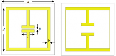
In order to reduce the Q factor and remain the same resonant frequency, we tapered the loop width to increase the inductance and increased the gap to decrease the capacitance of the ELC resonator. Figure 4 compares the original ELC resonator and the tapered one. The original structure we proposed has an ELC resonator and a ground plane, separated by the FR4 substrate with height of 3.2mm. The ELC resonator has the dimensions of a=15mm, g=0.4mm, d=12.6mm, b=0.8mm, l=3.6mm and copper thickness of t=0.035mm. The tapered resonator has the gap size varied from 0.4mm to 2.0mm and loop width decreased from 0.8mm to 0.1mm.
From Figure 5 illustrates the reflection coefficient S11 for the metamaterial absorber. The transmission coefficient is 0 because of the metal ground plane. It is interesting to note that the metamaterial absorber resonates at frequency of 2.4GHz with minimum reflection coefficient -18.75dB with the bandwidth is 0.0389GHz.
Figure 5 shows the changes in the bandwidth as the gap size increases from 0.4 to 2mm. We can conclude that the bandwidth increases as gap size g increases until 0.8mm, then the bandwidth keeps decreasing as gap size increases, which is completely different from the analysis about Q factor before. In addition, we can observe that the return loss at resonance also increases as the gap size increases.
The reason for the results mentioned above can be explained by using interference theory, which leads to the multiple reflection and transmission inside of the absorber structure. Figure 2 shows that the metamaterial absorber has 2 layers: resonator and ground plane. The overall reflection is the superposition of the multiple transmissions and reflections [12], which is defined as:
where φ1=∅12+∅21+∅23+2β, φ2=∅12+∅23+∅21+2β, β=-√(ε_FR4 ) k_0 d/cos(α_s), k0 is the free space wave number.
The formula demonstrates that the overall reflection is associated with the reflection and transmission coefficient of ELC resonator, the reflection coefficient of ground plane, the height of the substrate and the angle of incidence. Hence, the overall bandwidth of the reflection coefficient may be too small if we substitute all relevant values into the formula. Also, due to the complexity of the overall reflection, the bandwidth enhancement by structure tapering may not work for the metamaterial absorber since we only increased the bandwidth of the ELC resonator.
1.1.2 Substrate Height
We then investigated the impacts of the substrate height on the absorptivity and bandwidth. Based on the structure proposed in Section 4.1.1, we varied the substrate height from 2mm to 3.6mm.
Table 3 shows the bandwidth as the substrate height changes. It is interesting to note that the bandwidth starts with 0.0164 at 2.4GHz and increases until height increases to 2.8mm. Then the bandwidth start to decrease as the substrate height keeps increases. The optimized result we can obtain was 0.0398GHz, which is still relatively narrow. The reason for this can still be explained by the formula in section 4.11. Due to the complexity of the overall reflection, the bandwidth cannot be significantly improved by only changing the substitute height. In conclusion, the bandwidth still does not meet the specification although it can be slightly increased by varying the substrate height.
1.1.3 Via
After some unsuccessful trials, we finally presented the design of the metamaterial absorber operating at 2.4 GHz by using a via. A unit cell of proposed absorber is shown in Figure 7. It is a 3 layer structure which has a metallic loop at the top, a ground plane and a substrate in between. A 150Ω resistive load is used as a via to connect the top and bottom layer. The absorber is designed to operate at 2.4 GHz with the optimized dimensions given by a1=20mm, a=16mm, b1=19mm, b=13.4mm, w1=4, w2=2.6mm.
The unit cell was hosted on the top of a 3.2mm thick FR-4 dielectric substrate with a loss tangent of 0.025 and a dielectric constant of εr=4.4. The simulation for ELC resonator was performed with a full-wave electromagnetic simulator, Ansoft HFSS. The unit cell was placed in a waveguide with Master and Slave boundary condition. The boundary condition was selected for the unit cell in order to realize TEM mode excitation with polarization shown in Figure 7.
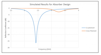
Figure 7 illustrates the performance of the absorber for both co-polarized direction and cross-polarized direction. From the graph, it is obvious that the absorber resonates at 2.4 GHz with reflection coefficient S11 of -26.3 dB for the co-polarization direction. In the meanwhile, the reflection coefficient for cross-polarization is 0 dB at 2.4 GHz. Using scattering parameters, the absorptivity is calculated by A=1-|S11|^2-〖|S21|〗^2, where S21 is 0 due to the ground plane. Therefore, the absorption rate is 99.77% based on the simulation results.
In addition, it is interesting to note that the bandwidth of the metamaterial absorber has been significantly increased to 0.2 GHz, which is 7 times more than that of the original design.
The reason why the design can successfully absorb power can be analysed by the surface current distribution, as shown in Figure 8. From the graph, we can observe that the surface current is mainly distributed at the middle of the left and right side of metallic loop. Meanwhile, the surface current at the top and bottom is minimal. However, the voltage at the surface will be distributed conversely. The voltage at top and bottom of the metallic loop is maximum while that at middle of left and right side is minimum. Therefore, connecting the top layer and ground plane with a resistive load enables the current to flow through the resistor due to the voltage difference, resulting in the power dissipation.
2.Experiment & Result
2.1 Absorber Test
Based on the simulated unit cell structure, a 10×10 metamaterial absorber array has been fabricated, as shown in Appendix B. The unit cells were hosted on the FR4 substrate with height of 3.2mm. The copper thickness for top and bottom layers is 0.035mm. The experiment was conducted in the Anechoic Chamber in order to mitigate the interference from the environment. Figure 11 demonstrates how the experiment was conducted in the Anechoic Chamber. To measure the absorption capability of the absorber, a pair of horn antennas, severing as transmitter and receiver of the power, was placed separately by the distance of 40 cm and connected to the Agilent N5230A analyser with low loss cables.
The absorber was placed in middle front of the 2 antennas. In order to ensure the accuracy of the measurement, the distance between the absorber and the antennas was 140 cm to avoid the near-field effects. However, the transmitting and receiving antennas would have incident angle of 8.13º with respect to the surface of the absorber plane due to the experiment limitations.
Firstly, we measured the power reflected by a copper sheet which has the same size as the absorber. Then, we tested reflection response by substituting the absorber for the copper sheet. The difference between two power responses can be considered as the absorption rate of the metamaterial absorber. The measured results are shown below:
Table 4 summarises the simulated and experimental results for the absorber at co-polarized direction. It is obvious that bandwidth, reflection coefficient and absorptivity for both are similar to each other. However, it is interesting to note that the resonant frequency for the measurement is 2.52 GHz, which is different from the simulated one.
Figure 11 shows the reflection coefficient for the cross-polarized direction. We can observe that the reflection coefficient for both simulation and measurement is 0 at 2.4 GHz, which means the absorber can reflect 100% incident power when cross-polarized. In addition, both results show that the resonant frequency at around 3.25 GHz. The difference between simulated and measured minimum reflect coefficients may result from the unwanted edge scattering caused by the finite array of unit cell
Discussion
From the results related to the absorber, we can conclude that the simulated results are very close to the measured ones except for the resonant frequency. The simulated resonant frequency is 2.4 GHz while the measured one is actually 2.52 GHz. This section will include a detailed discussion on the discrepancy between 2 resonant frequencies. The final design uses a 150 ohm resistor as a via to connect the top and bottom layer. In the fabrication process, the resistor we used is called MMA 0204, which is one of the professional thin film MELF resistors.
The RF behaviour of the MMA 0204 is illustrated in Figure 12. It is clear that MMA 0204 is purely resistive until 0.6 GHz. After that, the ratio of the total impedance to the resistance significantly increases beyond 1, which means the resistor will have capacitance or inductance at high frequency. From the graph, we can find that |Z|/R is roughly 1.7 at frequency of 2.4 GHz. Hence, the total impedance Z of the resistor at 2.4 GHz is given by:
Z=R(1+1.375j), where R is 150Ω
Accordingly, we need to consider the RF behaviour of MMA 0204 at 2.4 GHz in new simulation to obtain more accurate results.
Figure 13 shows the simulated S11 with RF behaviour considered and all results are summarised in Table 5. We can clearly see that resonant frequencies for the simulation and measurement are very close to each other, which means the resistor could be the potential reason which causes the resonant frequency shift.
Antenna Design
1.Method
This section is related to antenna design method and will introduce two failed methods and a successful method that is able to reduce the coupling between two antennas less than -40dB. The absorber design method and software algorithm will be introduced in latter section.
1.1 Antenna structure design method
According to the project requirement, transmission and receiving antennas should be on same side. So the dual patch antennas are decided for this project. The dual patch antennas should be built on same substrate and one is used to receiving and another one is used to transmission. So the antennas structure should be designed at first. The dimensions of the microstrip path antenna are determined by following parameters:
- Dielectric constant of substrate (εr)
- Thickness of substrate (h)
- Resonance frequency of antenna (f)
Based on the three parameters above, the dimension of microstrip patch antenna can be determined. So there are four key parameters are calculated and used for simulation in HFSS.
- The length (L) of the patch
- The width (W) of the patch
- The width (W0) of the feed line
- The length of rectangle (y0) which should be substrate on patch
1.2 Reducing coupling method
Using the ‘U’ shape structure between two patch antennas. From figure 6, this method is also cutting slots on ground plane between two same directional patch antennas and the ‘U’ shape is composed of three slots. The principle of the ‘U’ shape structure is based on an isolation of reverse phase coupling for reducing coupling.
2. Antenna results
2.1 Design calculation result:
As referred above, in order to increase the bandwidth of antenna, the RT/duroid 5880 has been chosen as substrate. The substrate parameters and the desired resonance frequency of the antenna are as follow:
- Dielectric constant of substrate εr is 2.2
- Thickness of substrate h is 1.6mm
- Resonance frequency f is 2.4GHz
According to the calculation methods from the Balanis, the dimension of microstrip line patch antenna can be determined based on above the parameters.
- The length (L) of the patch
- The width (W) of the patch
- The width (W0) of the feed line
- The length of rectangle (y0) which should be substrate on patch
2.2 Simulated and measured result
This section includes single antenna, dual patch antennas without ‘U’ structure, and dual patch antennas with ‘U’ structure. Each situation contains simulated result, measured result and comparison as well as relevant discussion.
- Single patch antenna:
The Figure below illustrates the reflection coefficient at resonate frequency 2.4GHz. The S11 is around -23.78dB at resonance frequency 2.4GHz, which means nearly 99.3% energy has been transmitted through the patch antenna. The reflection coefficient is lower and the input impedance match the transmission line. So the input impedance is close to 50 ohms.
- Dual patch antennas (Without ‘U’ structure):
Due to large power drop by using single antenna receiving and transmission, the dual patch antenna is introduced. In the dual patch antennas system, one antenna is used to receiving and another one is used to transmission simultaneously. The following figures illustrate simulated results of reflection coefficient S11 and coupling effect S21 of dual patch antenna without ‘U’ structure.
Simulated result:
Measured results:
The following figures illustrate measured results of reflection coefficient S11 and coupling effect S21 for dual patch antennas.
Comparison:
From figures above, comparing simulated result of reflection coefficient S11 that is around -19dB at resonance frequency 2.4GHz with measured result of reflection coefficient S11 that is -18dB at 2.4GHz, it is obviously that the simulated result is very close to measure results and the resonate frequency is in ISM frequency bandwidth. The S11 result is acceptable. The most important characteristic for the project which should be improved is crosstalk. From figures above, comparing the simulated result of crosstalk coefficient S21 that is around -19dB at resonate frequency 2.4GHZ with measured one which is around -23dB at resonate frequency. The coupling between two patch antennas is too large for the project to accept since it will have large effect on receiving.
- Dual patch antennas with ‘U’ structure:
Using ‘U’ structure between two antennas, the following figures illustrate simulated result of reflection coefficient and coupling effect as well as measured. The figure 20 and figure 21 illustrate prototype of dual patch antennas with ‘U’ structure
Comparison:
From figure 19, after using ‘U’ structure between two patch antennas, the reflection coefficient of simulated is around -19dB at resonate frequency 2.4GHz and measured reflection coefficient is around -24dB at 2.4GHz. Those two results are similar with each other and the performance is acceptable. For the crosstalk efficient, the crosstalk efficient of simulated at resonate frequency is around -43.3dB and the measured crosstalk efficient is -45dB at 2.4GHz. Those two result are close to each other and it is obviously that the coupling between two patch antennas has been reduced dramatically compared with the without ‘U’ structure case. Also from the figure 15, the simulated curve of reflection coefficient overlap the measured one and crosstalk curve of simulated and measured are also similar with each one. The performance of dual patch antennas has met the requirement. The details of principle of ‘U’ will be discussed in next section.
From figure 22 to figure 24, they demonstrate measured radiation pattern for two patch antennas with ‘U’ structure. All the radiation patterns were measured in the echoic chamber. The two patch antennas system was measured from -180 degree to 180 degree and the measured frequency at 2.4GHz with 1601 sweep points. From the figure 23, it is obviously that the maximum gain in E-plane and H-plane are at 0 degree. So the performance is acceptable and this design has satisfied with the requirement of the project.
Results summary:
Single patch antenna:
Dual patch antennas without ‘U’ structure:
Dual patch antennas with ‘U’ structure:
Discussion:
This section will focus on some physical explanations about the ‘U’ structure and explain the reason why the ‘U’ structure can reduce the coupling between two patch antennas.
The most important target for this project is reducing the crosstalk between two patch antennas and keeping the antenna system in same plane. Comparing the dual antennas system with ‘U’ structure with antenna system without cut, the figure 25 clearly demonstrates that the coupling between two patch antennas has been reduced nearly 20dB at resonate frequency 2.4GHz no matter what simulation or measurement. The final measured result of coupling is around -45dB which is satisfied with requirement of project.
Actually there are a little bit errors between simulated S21 without ‘U’ structure and measured S21 without ‘U’ structure. The reason is the actual patch antennas system without ‘U’ structure was not fabricated. In order to realize this case, the project group stuck some copper slots to cover ‘U’ structure. So glue could a factor which can affect the measured results. However the errors are in a reasonable range so it is still acceptable.
As the figure 26 shows, the letter ‘a’ and ‘b’ represent height and width of a slot. Currently the best size of slot can be obtained through HFSS when a is equal to 46mm and b is equal to 2mm.
The principle of ‘U’ structure is based on an isolation technology of reverse phase coupling. Assuming the signal comes into left patch antenna. From the figure 25, the black arrow indicates the surface current direction in left antenna. Due to the interference between two antennas, this surface current in left antenna would effect on right one and cause a same direction surface current in right patch antenna. However if there is a ‘U’ structure between patch antennas, from the figure 25 the red arrows indicate the surface current flow direction in slots. It is clearly to see the current flowing in right arm is opposite direction compared with original surface current. This opposite direction surface current would cancel out the original coupling in right antenna. So that is the reason why the ‘U’ structure can be used to reduce coupling for strongly coupled antennas.
Software Design
The software design consists of 2 main parts. One is the calculation algorithm, which is responsible for calculating the rotation speed. The other one is the user interface, which is used to display the measured data to users. The main principle used for the calculation algorithm is Fast Fourier Transform (FFT). According to the discussion in Section 1.2, the reflected power shall periodically vary from 0 to maximum due to the polarization loss. Therefore, FFT transforms the received power in time-domain to frequency-domain and the fundamental frequency of the frequency-domain signal provides the information of the rotation speed. The calculation algorithm is reused from the previous design.
By contrast, the user interface is adapted this year to display different information. A 16×2 bit LCD keypad is connected to the Arduino UNO board. From Figure 27, it is interesting to note that there are 6 buttons available in the LCD keypad shield. However, only Left, Top, Bottom and Right are used for the message display.
The functionality of the user interface is listed as follows:
- The Greeting Message will be displayed on the screen at the beginning. The message begins with “Hi, Welcome” and “Group 28 Wireless Rotation Detector”, which shifts from right to left on the screen, then the students’ and supervisors’ information shows up.
- The display message can be skipped if “Left” button is pressed. The user interface will then display the rotation speed of objects if the greeting message display is skipped or ends.
- Pressing “Down” button at speed display enables user to read the information regarding power level. The LCD display will show the maximum and minimum power at the screen in dBm.
- Pressing “Up” button at Power display will make software display the rotation speed again.
- The “Right” is used to restart the software system.
Entire System Test
The system test was performed after the absorber and antenna test have been completed. Figure 23 shows the experiment for the system test. We attached the absorber on the centre of a wheel driven by the DC power supply. The dual antennas were hosted at the front part of the housing while the remaining components were mounted on the base.
The purpose of the system test is to test the performance of the entire system from 2 aspects including accuracy and operating distance.
In order to measure the accuracy of the system, a tachometer has been used as a reference. We randomly picked 10 cases which had different rotation speeds, then we measured the speed by using the tachometer and the system we constructed. Finally, we compared the difference between 2 measurements to determine if the system was accurate enough.
For the operational distance test, we made the wheel spin at a fixed speed, then we gradually moved the antennas away from the absorber until “No Connection” was displayed on the screen. Meanwhile, the distance between the antenna and absorber could be considered as the maximum operational distance.
Table 11 shows the results measured by the tachometer and the constructed system. It is clear that the results are very close to each other with the maximum error only 3.3%, which means the system has satisfied the requirement of accuracy.
Table 12 provides the information about the operational distance. From the table, it can be concluded that the maximum distance for the system is roughly 70 cm. Given that the operating distance for the original system was 57 cm [2], the system has already been improved from the respective of the operating distance.
Conclusion
The thesis provides the information about the introduction, system design, experiment and result analysis of the wireless rotation detector project. The main objective of this year project is to enhance the performance of the absorber and modify the structure of antenna. For the absorber design, the metamaterial absorber has the resonant frequency at 2.52 GHz with 99.68% absorptivity. The bandwidth of the absorber is 0.17 GHz, which has been significantly enhanced compared to the simulated result (0.03 GHz) from last year. The potential cause for the resonant frequency shift is also discussed in section 6.1, so current structure of the absorber can be modified with the consideration of resistors’ RF behaviour in order to achieve 2.4 GHz resonant frequency. Overall, the absorber design has successfully met the specifications we proposed at the beginning of the project.
On the part of antenna design, the performance of dual patch antennas is acceptable for our project. The reflection coefficient of dual patch antennas is around a low value at resonate frequency and ensure more than 90% power can be transmitted. The challenge for antenna design is keeping the antenna system in a plane and reducing the coupling less than -40dB. So the isolation technology of a reverse phase coupling has been introduced. So this technology has reduced the coupling between two patch antennas less than -40dB, which can ensure that the transmitting signal would not affect the reading.
The requirements about the accuracy and the operating distance of the entire system have also been reached. The entire system can measure the rotation speed within 4% error compared to the commercial product, Tachometer. In addition, the operating distance is also increased from 57 cm to 70 cm under test environment. Overall, the objectives of the project have been achieved and the entire system could be useful for future industrial applications.
Reference
[1] C.A Balanis, “Antenna Theory Analysis and Design”, 3rd ed., New York: Wiley, 2005.
[2] “Arduino FFT Library”, openmusiclabs, Available: http://wiki.openmusiclabs.com/wiki/ArduinoFFT.
[3] D. Schurig, J.J. Mock, and D. R. Smith, “Electric-filed-coupled resonators for negative permittivity metamaterials”, Appl. Phys. Lett. 88, art. no. 041109(2006).
[4] Y. Chen, “Wireless Rotation Detector for Sport Equipment”, 2014.
[5] T. Mark, “System Overview,” Wireless Rotation Detector for Sport Equipment, 2014, pp 6-8.
[6] H. M. Lee, “Absorption Bandwidth-Enhanced Metamaterial absorber Using In-planed ELC resonator and Cut-Wire,” available: http://ournal.sapub.org/eee [Accessed: 22 March 2015]
[7] A. Grasso, Notes of Project Management for Electrical Engineering & Sustainable Energy, 2014. [Online]. Available: https://myuni.adelaide.edu.au/bbcswebdav/pid-5997024-dt-content-rid-6342045_1/courses/3420_ELEC_ENG_COMBINED_0001/Project%20Management%20%283024%20%26%203029%29%20Lecture%20Notes_2014.pdf
