Difference between revisions of "Projects:2015s1-28 Wireless Rotation Detector"
(→Antenna Design) |
(→Metamaterial Absorber Design) |
||
| Line 266: | Line 266: | ||
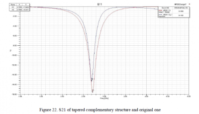
Figure 22 shows the simulated return loss of the tapered complementary structure with increased gap g =1.9mm and decreased loop width b=0.3mm. Note that while tapering the complementary structure decreases the equivalent inductance, decreasing the gap size increasing the equivalent capacitance, thus the resonant frequency for the tapered complementary resonator can be remained identical with the original design. However, compared to the original design, the tapered resonator has benefits in terms of the bandwidth. As demonstrated in the formula above, the simulated result shows that the tapered complementary resonator presents stronger resonance with bandwidth of 0.187GHz (in red line), which is 62.6% wider than the original one (0.115GHz in blue line). | Figure 22 shows the simulated return loss of the tapered complementary structure with increased gap g =1.9mm and decreased loop width b=0.3mm. Note that while tapering the complementary structure decreases the equivalent inductance, decreasing the gap size increasing the equivalent capacitance, thus the resonant frequency for the tapered complementary resonator can be remained identical with the original design. However, compared to the original design, the tapered resonator has benefits in terms of the bandwidth. As demonstrated in the formula above, the simulated result shows that the tapered complementary resonator presents stronger resonance with bandwidth of 0.187GHz (in red line), which is 62.6% wider than the original one (0.115GHz in blue line). | ||
| + | |||
| + | |||
| + | 1. Method | ||
| + | |||
| + | |||
| + | 1.1 Metamaterial Absorber Design | ||
| + | |||
| + | |||
| + | According to the introduction given in the Section 1.3, the existing absorber can only absorb 36% of incident power at 2.4 GHz when it has the same polarization with the antenna. The main cause for this is that the bandwidth of the existing metamaterial absorber is only 0.03 GHz, which is too narrow. As a consequence, the performance of the absorber will significantly drop if the resonant frequency slightly shifts. Accordingly, the main purpose for the new absorber design is to achieve distinct absorption performance and relatively wide bandwidth. | ||
| + | This section will demonstrate some different methods which have been tried to increase the bandwidth of the absorber. | ||
| + | |||
| + | |||
| + | 1.1.1 Structure Tapering | ||
| + | |||
| + | |||
| + | In section 3.13, we presented the characteristics of ELC resonator and its equivalent circuit. The ELC resonator can be modelled as a parallel LC resonator and the resonant frequency can be adjusted by changing resonator’s dimensions. In order to enhance the bandwidth, we need to consider the impact of the Q factor. For a parallel RLC circuit, the Q-factor is defined as | ||
| + | |||
| + | |||
| + | |||
| + | |||
| + | Q=R√(C/L) | ||
| + | |||
| + | |||
| + | And the bandwidth can be expressed as | ||
| + | |||
| + | BW=f_r/Q | ||
| + | |||
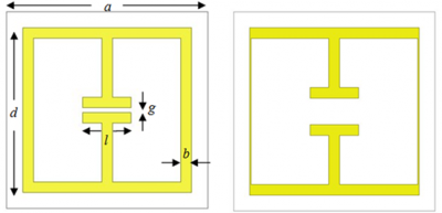
| + | In order to reduce the Q factor and remain the same resonant frequency, we tapered the loop width to increase the inductance and increased the gap to decrease the capacitance of the ELC resonator. Figure 4 compares the original ELC resonator and the tapered one. The original structure we proposed has an ELC resonator and a ground plane, separated by the FR4 substrate with height of 3.2mm. The ELC resonator has the dimensions of a=15mm, g=0.4mm, d=12.6mm, b=0.8mm, l=3.6mm and copper thickness of t=0.035mm. The tapered resonator has the gap size varied from 0.4mm to 2.0mm and loop width decreased from 0.8mm to 0.1mm. | ||
| + | |||
| + | [[File:ELC_resonator_and_tapered_one.PNG|400px|thumb|center|alt text]] | ||
== Antenna Design == | == Antenna Design == | ||
Revision as of 12:27, 22 October 2015
Contents
Supervisors
Honours students
- 2015: Guowei Deng and Shuopeng Wang
Project objects
Scope
- Design and construct a portable wireless device which can accurately measure the speed of rotating object.
Specific Aims
The aim of the project is to design and construct a portable wireless device which can be used for rotation speed measurement. The device is supposed to consist of antennas, absorbers, Arduino UNO Board with software, etc. The outcomes of the project will be as follows:
- A metamaterial absorber with resonant frequency of 2.4GHz
- A planar dual-antennas with capability of transmitting and receiving signals
- A software system for rotation speed calculation
The device should be able to measure the rotational speed of various objects such as sport equipment, car tyres, turbines, fans, etc. The system shall be operational under a set of circumstances and able to achieve reliable results.
Background & Significance
- Motivation
The rotation speed measurement devices have already ubiquitously used in industries. They are embedded on turbines, wheels or fans to extract the rotation speed of objects. However, most of commonly used angular speed measurement devices, such as laser tachometer, use visible light. One of the constraints in such devices is that the line of sight cannot be impaired [1]. Hence, the optical devices cannot be used if there is an obstacle between rotating objects and the test devices or under sophisticated circumstances such as fog or smoke.
In order to improve the performance of the measurement device, the 2.4GHz electromagnetic waves will be used instead of visible light due to its good ability of propagation. Accordingly, the devices can be used under more complicated situations, even if the line of sight has been impaired, once delivered.
- Technical Background
1. Polarization of Antennas
The polarization of antenna is defined as “the polarization of the wave transmitted (radiated) by the antenna” [2]. There are 3 different types of polarization including linear polarization, circular polarization and elliptical polarization [2]. All of them are defined as “time-varying direction and magnitude of the electric field vector” [2].
2. Polarization Loss Factor
Polarization loss is defined as the power loss due to polarization mismatch. For example, if a horizontally polarized antenna communicates with a vertically polarized antenna, the vertically polarized antenna will transmit vertically polarized waves, while the horizontally polarized antenna can only receive horizontally polarized wave. Thus, there is no power transfer between a horizontally polarized antenna and vertically antenna according to the reciprocity principle. In contrast, if 2 vertically polarized antennas communicate with each other, the power transfer will be maximum. Hence, if two linearly polarized antennas are rotated from each other by an angle θ, the polarization loss factor base on power loss for polarization mismatch is defined as
𝑃𝐿𝐹 = 𝑐𝑜𝑠2θ
3. Metamaterial Absorber
Metamaterials are man-made materials with the unique characteristics, such as negative permittivity and permeability, which cannot be found in natural materials [3]. The metamaterial absorber has been one of the most important applications due to its astonishing properties [4]. A single metallic metamaterial absorber typically consists of a LC resonant circuit and a ground plane, separated by a substrate in between [5]. For example, as shown in Figure 1, the capacitor-like structure can provide capacitance and is connected with two loops in parallel, which can be considered as two inductors in the resonant circuit [6]. The resonator can strongly respond to a properly oriented electric field due to the capacitor-like structure when the circuit is driven by EM field at resonant frequency.
The metamaterial absorber is expected to have the ability of dissipating the incident waves inside of the structure with limited energy reflected back from it [8]. As shown in Figure 2, the incident wave is transmitted into the substrate at working frequency. The surface current will be created along the ground plane when the wave reached the bottom layer. Similarly, remaining energy will be reflected back to the resonators which will also generate another surface current on the top layer. These two currents have same magnitude with opposite directions, resulting in a destructive interference [8]. Hence, the thickness of the substrate should be carefully chosen for the effective destructive interference.
Key Requirements
From the introduction of background and related work, several key requirements have been defined as following:
- Metamaterial absorber shall absorb at least 90% (-10db) power at 2.4GHz when it has
same polarization as the transmitting antenna.
- Dual antennas shall work at 2.4GHz and crosstalk between 2 antennas shall be less
than -40dB.
- Portable system shall be operational up to 50cm from the rotating object.
- Portable system shall accurately measure the angular speed of the rotating object in
both low and high speed.
- While the mutual coupling in dual antennas is reduced, the dimensions of dual antenna
should remain small, and specifically the antenna system should be planar.
- The bandwidth for the isolation should be able to cover the bandwidth of the antenna.
Technical Challenge
- Antenna Design
The technical challenge for antenna design is to figure out an appropriate method to reduce crosstalk between dual antennas with the frequency and substrate thickness specified. Some possible methods have already been mentioned in Section 3.2.2. However, all the methods will have side effects on the performance of the antenna including input impedance matching, efficiency, resonant frequency, etc. Hence, the method should be operational for coupling reduction with all side effects minimized. Furthermore, the method should not dramatically change the overall dimensions of the antenna, and specifically the antenna system is expected to be planar.
- Metamaterial Absorber
Resonant frequency and absorption ability are two key characteristics of the metamaterial absorber, which are influenced by the metallic structure and thickness of substrate. Hence, 2 variables need to be considered in absorber design in order to achieve the requirements. Moreover, the material of substrate is supposed to be FR4, a low-cost material with permittivity varying from 4.2 to 4.8. The variation of the permittivity has impact on the resonant frequency, which may lead to failure in absorber design. Hence, a relatively wide bandwidth has to be achieved in order to overcome the uncertainty.
Proposed Approaches
- Method exploited - ‘Divide-And-Conquer’.
- The entire project can be decomposed into several aspects.
- Hardware (design required)
- Metamaterial Absorber
- Dual-Antennas
- Software
- Calculation Algorithm for rotating speed
- GUI
- Other Components (from market or school)
- VCO
- Arduino UNO Board
- Power Detector
Hardware Design
Hardware design will begin with understanding the key requirements and specifications of the hardware. Most of the hardware design will be implemented in the commercial software package HFSS which is a professional software for simulating 3D full wave electromagnetic fields. The group member will fabricate the designed hardware after hardware has been designed in HFSS. The next task for hardware is to measure the prototype and compare the practical result with simulation results. If the prototype fails to meet the requirements, the group will refer back to design stage to redesign prototype until it meets requirements
Software Design
The software design will start after antenna and absorber design have been finished. The software design will be in C language based on the Fourier Transform. To test the validity of the software, the group members will combine software, hardware and other components together. If the software cannot accurately measure rotating speed of objects which is driven by a motor, the project group will return to previous stage to redesign the software.
Schedule and Milestone
- Milestone in Semester 1
- Milestone in Semester 2
Metamaterial Absorber Design
1.Electrical-LC Resonator
A typical electrical-LC resonant circuit was illustrated in Figure 1. In order to investigate the characteristics of the Electrical-LC resonator, we proposed a simple structure with dimensions of a=15mm, g=0.4mm, d=12.6mm, b=0.8mm, l=3.6mm and copper thickness of t=0.0035mm, as the dimension of the structure shown in Figure 1. The unit cell was hosted on the top of a 3.2mm thick FR-4 dielectric substrate with a loss tangent of 0.025 and a dielectric constant of εr=4.4. The current structure did NOT include the ground plane at the bottom because we only investigated the characteristics of the ELC resonator at this stage.
The simulation for ELC resonator was performed with a full-wave electromagnetic simulator, Ansoft HFSS. The unit cell was placed in a waveguide with Perfect Magnetic Conductor and Perfect Electric Conductor assigned in x-z plane, y-z plane respectively. The boundary condition was selected for the unit cell because of its symmetric structure with symmetric wave propagation. Figure 1 shows the reflection coefficient S11 and transmission coefficient S21 at the frequency ranging from 1 to 5GHz.
From Figure, we can observe that S11 has the resonant frequency at 3.16GHz with the magnitude of -16.22dB while the S21 resonates at 2.75 GHz with magnitude of -23.31dB. It is interesting to note that the S11 reaches the maximum value when S21 reaches the minimum 19 value and vice versa. This is because the relationship between S11 and S21 can be expressed as |𝑆21|2=1−|𝑆11|2 using scattering parameters. Moreover, we can observe that the bandwidth for S11 is 0.1152GHz and for S21 is 1.207GHz. In proposed design, a number of factors played a key role in determining the resonant frequency. The resonant frequency of a RCL circuit can be defined as
𝑓𝑟=12𝜋√𝐿𝐶
Thus, the most important factors to determine the resonant frequency are capacitance and inductance. The capacitance is affected by the dimensions of the capacitor-like structure including capacitor length l and gap g while the inductance is determined by the dimensions of the loops including the unit cell size d and width b. Hence, we used the “Optimetrics” in HFSS in order to figure out the effects of these 4 parameters.
1.1. Length l
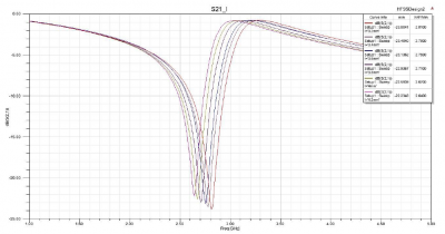
By varying the length l of the capacitor from 3.2mm to 4.2mm, we sought to observe the effect of the range on the resonant frequency. It is beneficial in context of our project as it demonstrates the effects of the capacitance on the resonant frequency.
From Figure, we can observe that the resonant frequency of the ELC circuit decreases from 2.81GHz to 2.64GHz as a result of the increment of length l from 3.2mm to 4.2mm. The decreasing of the resonant frequency indicates that the capacitance increases as we increase the length l. This phenomenon can be explained by using the formula of parallel plate capacitor:
𝐶=𝜀𝐴/𝑔
The capacitance of parallel metallic plates of area A and separation g is given by the expression above where ε= permittivity of space between two plates. As we increase the length l of the capacitance, the area A increases and the capacitance increases as well. Accordingly, the resonant frequency will decrease.
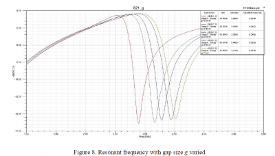
1.2. Gap g The air gap g was varied from 0.2 to 1mm by step 0.2mm. Figure 8 illustrates the variations of the resonant frequency as the air gap increases from 0.2mm to 1mm.
It is clear from Figure 8 that the resonant frequency of the resonator remarkably increases as the gap increases. This phenomenon can be explained by the formula in previous section: the capacitance decreases as the air gap increases and the resonant frequency will increase as a result.
We can also observe the coupling strength decreases if the capacitance is increased. Weak coupling has the undesired effects of narrow bandwidth, as shown in Figure 8 where the bandwidth decreases as gap g decreases.
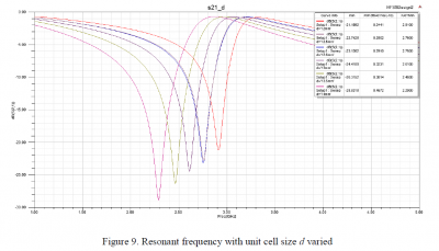
1.3. Size d The inductance of the RCL circuit is directly dependent on the size of the unit cell. By examining the resonant frequency from different sizes of unit cell it allows us to predict further resonator characteristics.
We can also observe the coupling strength decreases if the capacitance is increased. Weak coupling has the undesired effects of narrow bandwidth, as shown in Figure 8 where the bandwidth decreases as gap g decreases.
The above Figure 9 shows that the resonant frequency keeps increasing, which means the inductance of the ELC resonator keeps increasing as the size increases. Thus, we can directly adjust the resonant frequency by selecting the proper size of the unit cell.
1.4. Loop Width b
The variable presented in Figure 10 is called “cut-off”, which represents the width cut from the original loop. The “cut-off” increases from 0.1 to 0.7mm, which means the loop width decreases from 0.7 to 0.1mm. From Figure 10, it is obvious that the resonant frequency decreases as the width decrease, which indicates the narrower width the loop is, the higher inductance the loop has.
2.1 Bandwidth Enhancement of ELC Resonator
Bandwidth is the parameter which describes a range of frequency where the resonator can reflect or transmit electromagnetic field. The bandwidth is important in the metamaterial absorber design because of the property of the substrate. The FR-4 is a lossy material whose relative permittivity varies from 4.2 to 4.8, so the absorber is likely to be out of band if the bandwidth is too narrow.
In order to enhance the bandwidth, we need to consider the equivalent circuit illustrated in the Figure 1, which shows that the proposed ELC resonator can be modelled as RLC circuit in parallel. For a parallel RCL circuit, the Q factor is defined as
𝑄=𝑅√𝐶/𝐿
And the bandwidth can be expressed as
𝐵𝑊=𝑓𝑟/𝑄
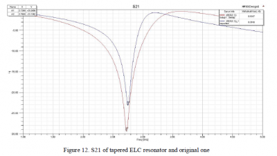
In order to reduce the Q factor and remain the same resonant frequency, we tapered the loop width to increase the inductance and increased the gap to decrease the capacitance of the ELC resonator. Figure 11 compares the original ELC resonator and the tapered one, the tapered resonator has the gap size increased from 0.4mm to 1.9mm and loop width decreased from 0.8mm to 0.1mm.
Figure 12 shows the simulated transmission coefficient of the tapered ELC resonator with increased gap g=1.9mm and decreased loop width d=0.1mm. Note that while tapering the ELC resonator increases the equivalent inductance, increasing the gap size decreases the equivalent capacitance, thus the resonant frequency for the tapered resonator can be remained same as the original design. However, compared to the original design, the tapered resonator has benefits in terms of the bandwidth. As demonstrated in the formula above, the simulated result shows that the tapered ELC resonator exhibits stronger resonance with bandwidth of 0.5GHz (in red line), which is 72.4% wider than the original one (0.29GHz in blue line).
2.2 Metamaterial Absorber
In section 2 and 2.1, we presented the characteristics of the ELC resonator and a method to enhance its bandwidth. The ELC resonator can be modelled as a LC circuit and the resonant frequency can be affected by its dimensions. Moreover, the tapering method circuit enables us to significantly increase the bandwidth and reduce the electrical area of ELC circuit. Based on the results analysed in previous sections, we proposed a structure for a metamaterial absorber that has ECL resonator and a ground plane, separated by the FR4 substrate with height of 3.2mm in between. The dimension of the ECL resonator is identical to the previous one in Section 2.
Figure 13 illustrates the reflection coefficient S11 for the metamaterial absorber. The transmission coefficient is 0 because of the metal ground plane. It is interesting to note that the metamaterial absorber resonates at frequency of 2.4GHz with minimum return loss -18.75dB. The bandwidth is 0.0389GHz, which is roughly only 1/10 of that of the single resonator shown in Figure 13.
The method discussed in Section 2.2 was then used in order to increase the bandwidth of the metamaterial absorber. Similarly, we tapered the loop width into 0.1mm and decreased the gap size to reduce to investigate the variation in bandwidth.
Figure 14 shows the changes in the bandwidth as the gap size increases from 0.4 to 2mm. We can conclude that the bandwidth increases as gap size g increases until 0.8mm, then the bandwidth keeps decreasing as gap size increases, which is completely different from the result found in section 2.2. In addition, we can observe that the minimum value of the return loss also decreases as gap size increases.
The reason for the results mentioned above can be explained by using interference theory, which leads to the multiple reflection and transmission inside of the absorber structure. Figure 2 shows that the metamaterial absorber has 2 layers: resonator and ground plane. The overall reflection is the superposition of the multiple transmissions and reflections, which is defined as:
𝑟=(𝑟12𝑒^𝑖∅12−𝑟12𝑟21𝑟23𝑒^𝑖𝜑1+𝑡12𝑡21𝑟23𝑒^𝑖𝜑2)/(1−𝑟21𝑟23𝑒𝑖(∅21+∅23+2𝛽)) where 𝜑1=∅12+∅21+∅23+2𝛽, 𝜑2=∅12+∅23+∅21+2𝛽, 𝛽=−√𝜀𝐹𝑅4𝑘0𝑑/cos (𝛼𝑠), k0 is the free space wave number.
The formula demonstrates that the overall reflection is associated with the reflection and transmission coefficient of ELC resonator, the reflection coefficient of ground plane, the height of the substrate and the angle of incidence. Hence, the overall bandwidth of the reflection coefficient may be the 1/10 of the original one if we substitute all relevant values into the formula. Also, due to the complexity of the overall reflection, the bandwidth enhancement method may not be working for the metamaterial absorber since we only increased the bandwidth of the ELC resonator.
2.3 Complementary Shape
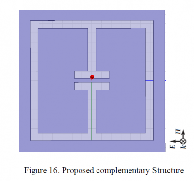
Section 2.2 concludes that the bandwidth of the metamaterial absorber will be significantly reduced compared to the single ELC resonator and the method to increase the bandwidth is not operational for the metamaterial absorber. In order to achieve relatively wider bandwidth, another structure called “complementary shape” was proposed. Complementary shape is the structure designed by cloning the ELC resonator to a copper sheet so that the ELC resonator structure will be a hole instead of copper, shown in Figure 16. The dimension of the complementary shape is also same as previous ELC resonator.
In order to investigate the property of the complementary shape, the structure was placed on the top of a FR4 substrate without the ground plane. The simulation was performed using waveguide whose directions of fields are shown in the Figure 16.
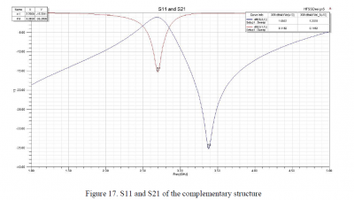
Figure 17 shows that S11 has the resonant frequency at 2.7GHz with the magnitude of -15.33dB while the S21 resonates at 3.38 GHz with magnitude of -35.28dB. These 2 scattering parameters also have relationship of |𝑆21|2=1−|𝑆11|2 due to the lack of ground plane. Moreover, we can observe that the bandwidth for S11 is 0.1152GHz and for S21 is 1.207GHz.
Similar to the analysis in Section 2, we also investigated the effects of the dimensions on the resonant frequency by varying each parameter.
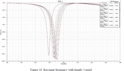
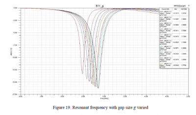
Figure 18 shows that the resonant frequency decreases when the length l increases. When we increase the length l, the size of the copper line in the middle also increases. This line can be considered as an inductor in the complementary circuit and the inductance increases as we increase the length, resulting in the resonant frequency decreasing. Similarly, the resonant frequency also decreases if we reduce the gap size g, as shown in Figure 19.
Figure 20 illustrates that the effects of loop width b on the resonant frequency. We can conclude from the Figure that the resonant frequency increases as the loop width b increases. This is because the increasing of the loop width b results in the decreasing of the capacitance so that the resonant frequency increases accordingly.
2.4 Bandwidth Enhancement of Complementary Shape
From the overview of the structure, the complementary structure can be modelled as RCL circuit in series, which is different from the original structure. For a series RCL circuit, the Q factor can be defined as
𝑄=1𝑅√𝐿/𝐶
And the bandwidth is determined by
𝐵𝑊=𝑓𝑟/𝑄
In order to reduce the Q factor and remain the same resonant frequency, we tapered the loop width to increase the capacitance and increase the gap to decrease the inductance of the complementary structure. Figure X compares the original complementary structure and the tapered one, the tapered resonator structure has the gap size g increased from 0.4mm to 1.9mm and loop width b decreased from 0.8mm to 0.3mm.
Figure 22 shows the simulated return loss of the tapered complementary structure with increased gap g =1.9mm and decreased loop width b=0.3mm. Note that while tapering the complementary structure decreases the equivalent inductance, decreasing the gap size increasing the equivalent capacitance, thus the resonant frequency for the tapered complementary resonator can be remained identical with the original design. However, compared to the original design, the tapered resonator has benefits in terms of the bandwidth. As demonstrated in the formula above, the simulated result shows that the tapered complementary resonator presents stronger resonance with bandwidth of 0.187GHz (in red line), which is 62.6% wider than the original one (0.115GHz in blue line).
1. Method
1.1 Metamaterial Absorber Design
According to the introduction given in the Section 1.3, the existing absorber can only absorb 36% of incident power at 2.4 GHz when it has the same polarization with the antenna. The main cause for this is that the bandwidth of the existing metamaterial absorber is only 0.03 GHz, which is too narrow. As a consequence, the performance of the absorber will significantly drop if the resonant frequency slightly shifts. Accordingly, the main purpose for the new absorber design is to achieve distinct absorption performance and relatively wide bandwidth.
This section will demonstrate some different methods which have been tried to increase the bandwidth of the absorber.
1.1.1 Structure Tapering
In section 3.13, we presented the characteristics of ELC resonator and its equivalent circuit. The ELC resonator can be modelled as a parallel LC resonator and the resonant frequency can be adjusted by changing resonator’s dimensions. In order to enhance the bandwidth, we need to consider the impact of the Q factor. For a parallel RLC circuit, the Q-factor is defined as
Q=R√(C/L)
And the bandwidth can be expressed as
BW=f_r/Q
In order to reduce the Q factor and remain the same resonant frequency, we tapered the loop width to increase the inductance and increased the gap to decrease the capacitance of the ELC resonator. Figure 4 compares the original ELC resonator and the tapered one. The original structure we proposed has an ELC resonator and a ground plane, separated by the FR4 substrate with height of 3.2mm. The ELC resonator has the dimensions of a=15mm, g=0.4mm, d=12.6mm, b=0.8mm, l=3.6mm and copper thickness of t=0.035mm. The tapered resonator has the gap size varied from 0.4mm to 2.0mm and loop width decreased from 0.8mm to 0.1mm.
Antenna Design
An antenna is a metallic device which can be used to transmit and receive radio waves [2]. In the proposed system, two linearly polarized antennas are placed closely to transmit and receive powers. The key requirements of the antenna are:
- Dual antennas shall work at 2.4GHz and crosstalk between 2 antennas shall be less than -40dB.
- While the mutual coupling in dual antennas is reduced, the dimensions of dual antenna should remain small, and specifically the antenna system should be planar.
- The bandwidth for the isolation should be able to cover the bandwidth of the antenna.
1. Dumb-bell-like structure In order to reduce mutual coupling and keep microstrip line patch antennas in low profile, the dumb-bell-like structure are introduced. Base on the designed dual patch antennas, the dumb-bell-like structure has been roughly designed at present stage for reducing mutual coupling but the structure still need be modified since the mutual coupling has not been reduced significant at resonance frequency. So the mutual coupling (S21) is simulated in HFSS.
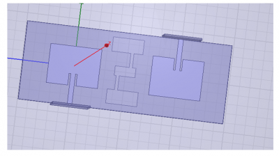
The above figure shows the designed dumb-bell-like structure that is used in current stage. The below table defines symbols for all parameters in dumb-bell-like structure.
Rectangle 1 Rectangle 2 Rectangle 3 Rectangle 4 Rectangle 5 Length a g W1 g a Height b I xi I b
2. Designed calculation result by using RT/Duroid 5880 There are three parameters which had been given before designed dimension of a microstrip line patch antenna.
- Dielectric constant of substrate (ℇr = 2.2).
- Thickness of substrate (h=1.6mm).
- Resonance frequency (f = 2.4GHz) of antenna.
The dimension of mircostrip line patch antenna can be designed base on above three parameters. So there are four key parameters were calculated and were required for simulate by HFSS.
- The length (L) of the patch.
- The width (W) of the patch.
- The width (W0) of the feed line.
- The length of rectangle (y0) which should be subtracted on patch
L=41.3481mm W=49.4106mm W0=4.5277mm Y0=12.8mm
3. Simulation result:
- Single patch antenna:
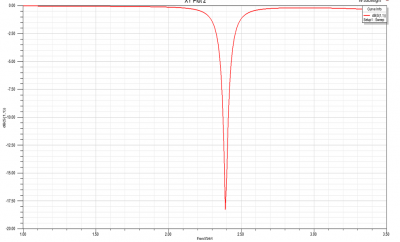
From the simulation result below, the return loss (S11) at 2.39GHz is -18.38dB for single patch antenna:
- Dual patch antennas:
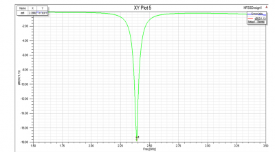
The return loss (S11) of dual patch antennas is -18.2dB at 2.39GHz.
- Reverse feeding dual patch antennas:
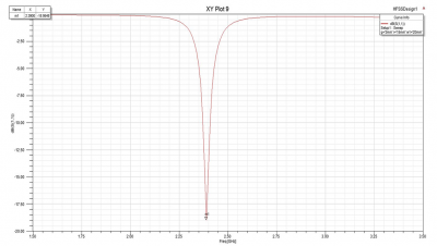
The return loss (S11) of reverse feeding dual patch antennas is -17.84dB at 2.39GHz
- Reverse feeding dual patch antennas with dumb-bell-like structure:
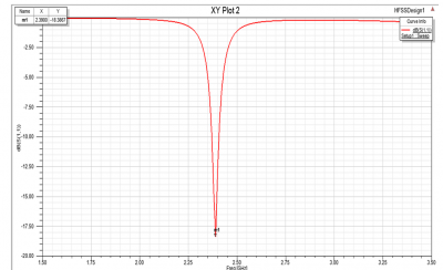
The return loss (S11) of reverse feeding dual patch antennas with dumb-bell-like structure is -18.96dB at 2.39GHz.
1. Antenna design Method
This section is related to antenna design method and will introduce two failed methods and a successful method that is able to reduce the coupling between two antennas less than -40dB. The absorber design method and software algorithm will be introduced in latter section.
1.1 Antenna structure design method
According to the project requirement, transmission and receiving antennas should be on same side. So the dual patch antennas are decided for this project. The dual patch antennas should be built on same substrate and one is used to receiving and another one is used to transmission. So the antennas structure should be designed at first. The dimensions of the microstrip path antenna are determined by following parameters:
- Dielectric constant of substrate (εr)
- Thickness of substrate (h)
- Resonance frequency of antenna (f)
Based on the three parameters above, the dimension of microstrip patch antenna can be determined. So there are four key parameters are calculated and used for simulation in HFSS.
- The length (L) of the patch
- The width (W) of the patch
- The width (W0) of the feed line
- The length of rectangle (y0) which should be substrate on patch
1.2 Reducing coupling method
The biggest challenge for antenna design is reducing the coupling between antennas less than -40dB and keeping antenna structure in a plane. In order to achieve this target, there are many different structures have been used.
- Using the dumb-bell-like structure between two reverse patch antennas.
From figure below, the ideal of this structure is cutting some slots on the ground plane which is at the bottom of antenna structure. The dumb-bell shape is composed of those slots.
Reference
[1] C.A Balanis, “Antenna Theory Analysis and Design”, 3rd ed., New York: Wiley, 2005.
[2] “Arduino FFT Library”, openmusiclabs, Available: http://wiki.openmusiclabs.com/wiki/ArduinoFFT.
[3] D. Schurig, J.J. Mock, and D. R. Smith, “Electric-filed-coupled resonators for negative permittivity metamaterials”, Appl. Phys. Lett. 88, art. no. 041109(2006).
[4] Y. Chen, “Wireless Rotation Detector for Sport Equipment”, 2014.
[5] T. Mark, “System Overview,” Wireless Rotation Detector for Sport Equipment, 2014, pp 6-8.
[6] H. M. Lee, “Absorption Bandwidth-Enhanced Metamaterial absorber Using In-planed ELC resonator and Cut-Wire,” available: http://ournal.sapub.org/eee [Accessed: 22 March 2015]
[7] A. Grasso, Notes of Project Management for Electrical Engineering & Sustainable Energy, 2014. [Online]. Available: https://myuni.adelaide.edu.au/bbcswebdav/pid-5997024-dt-content-rid-6342045_1/courses/3420_ELEC_ENG_COMBINED_0001/Project%20Management%20%283024%20%26%203029%29%20Lecture%20Notes_2014.pdf


