Projects:2020s2-7153 High-efficiency planar waveguides for terahertz waves
Abstract
Terahertz integrated systems are still in its infancy in terms of its technology. However, it has shown a great number of potential uses in communication, radar, imaging and sensing. This project aims to continue the study of waveguide by examining the dispersion, cross-polarization and crosstalk, along with the characteristics of bends and crossings over the 220 to 330 GHz (WR-3 band) operating frequency range. The waveguides are substrate-less effective medium with a subwavelength arrays of hole while supporting Ex11 and Ey11 modes with low loss and low dispersion. As a step to reduce significant absorption in metals and dielectrics at terahertz frequencies, the self-supporting structures are built by using a single silicon wafer.
Introduction
With a substantially growing proportion of the world's population accessing online services, data traffic has grown significantly. Most terahertz (THz) sources, however, are inaccessible, so designing efficient THz waveguides for versatile broadband THz radiation delivery is an important step towards terahertz techniques for practical applications. The terahertz spectrum that covers the frequency range from 0.1 to 10THz is an appropriate option for the support of the high-speed wireless sight transmission line by convergence electronics and optics. When used to connect the numerous THz point devices, such as sources, filters, sensor cells and detectors, THz waveguides can be very beneficial on system integration stage.
Project team
Project students
- Mahmoud Alshnqiti
- Muhammad Zulhisyam Mohd Hosni
- Muhammad Hairie Mohd Hamdan
Supervisors
- Dr. Withawat Withayachumnankul
- Dr. Wendy Lee
- Weijie Gao
Objectives
Due to its short wavelength, compared to microwave frequencies, terahertz frequencies have been recognized as a candidate to fulfill the high data traffic demands with attention to commercialize communications over the terahertz band [3].
The principle objective of this project to enhance the effective-medium-clad waveguides which is foreseen as a promising candidate for terahertz integrated circuits. Accordingly, we are enhancing the compactness of the platform by proposing a new bend design with smaller footprint. However, the main challenge is to decrease the footprint while maintaining high transmission, physical structure strength, and adhering the fabrication limitation.
Background
Terahertz background
The term terahertz (THz) is a prefix which refer to 1012. However, the terahertz domain typically defined as the frequencies from 100 GHz to 10 THz. The terahertz domain falls between the electronics and the photonics domains. The terahertz has special characteristics as it can penetrate plastic and fabric (e.g. dry clothes) and it's suitable for non-destructive imaging.
Effective medium cladding
Silicon has a high refractive contrast of n = 3.418 , allowing for high degree of confinement in the core via total internal reflections. By perforating cylindrical holes in a silicon wafer, with a small period compared to the wavelength, we could achieve an effective medium that has a refractive index between silicon and air. Figure 1 shows the model for the effective-medium-clad straight waveguide proposed by [1].
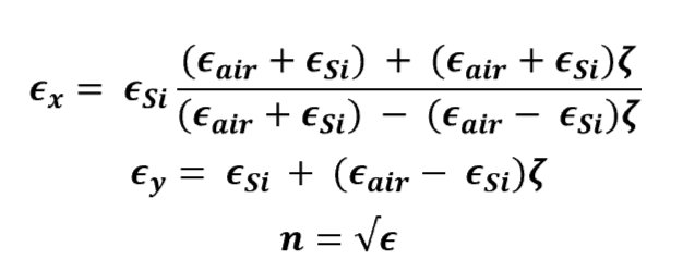
It's worth mentioning that the anitrpoic permettivy of he foundemtal modes are dependate on the mode in which it can approxmiated using Maxwell-Garnett approximation as shown in figure 2 [2].
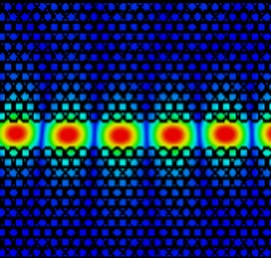
Figure 3, shows the waves concentrated in the core by total internal reflections with small exponential decaying penetration in the claddings.
Experimental demonstration of the effective-medium-clad waveguides
Since this wiki page doesn't allow embedding videos from external links, here is a link on the an experimental demostration of the usage of effective-medium-clad waveguies in the transmission of a uncompressed 4K video. video comprsseion is an method in which some algrothims, more likely fast motion estimation algrothims are used to decreased the data transmitted by only send the video frames portions that has changed. Therefore, we the video transmitted was not compressed.
- Here is the link to video on YouTube platform: https://www.youtube.com/watch?v=NtyunEEIOR4
Method
Similar to most RF related projects, the feedback of the quality of solutions proposed in this project are evaluated using a full-time software simulation package. Namely, CST software. In addition, after a satisfactory design simulations results, the design is sent oversees for fabrication. The process of fabrication is called deep reactive ion-etching (DRIE). The DRIE consitsts of a laser with high resolution that can make perforations into a slab of silicon with a diameter greater than 20μm.
Bend designs E-field plots
The e-field plots shows strong bend radiation in the standard bend with 0.75mm bend radius for both fundamental modes EY11 and EX11. On the other hand, the proposed bend design shows significant reduction in the waves radiating from the core which are also similar to the standard bend with 2mm bend radius.
Bend designs transmission coefficients (before normalization)
The transmission coefficients plots shows strong bend loss in the standard bend with 0.75mm bend radius for both fundamental modes EY11 and EX11. On the other hand, the proposed bend design shows significant reduction in the bend loss which have similar levels to the standard bend with 2mm bend radius. Hence, the animations and the transmission coefficients suggest improved bend loss with proposed bend design.
E-field simulation animations
As can be seen from the simulations, the standard bend has strong waves radiations in the core. On the other hand, the new proposed design has significantly decreased the radiation out of the bend structure.
Simulation Optimizer
Since the project outcomes rely heavily on the software simulator. We implemented a MATLAB program that could control the simulation tool and optimizer the design by making efficient use of time and computing resources. The optimizer analogy is shown in figure 9.
Results
Bending design outcomes
- Successfully decreased the bend design footprint by almost a factor of 3.
- The proposed bend design maintained high efficiency transmission in both fundamental modes EX11 and EY11.
- We proposed equations that can be used for designing waveguides bends universally.
More importantly, the principle outcome of this project is that we proposed a novel bend design that can achieve high transmissions and is simple to implement in which we anticipate to be greatly beatifical for researchers in photonics.
Bending design method
A new method for designing sharp and compact bends are proposed in this project. The method is expected to have a great potential due to the high efficiency in effective-medium-clad bending designs and it's implementation simplicity which might be useful in other photonic integrated circuits.
Note: The new proposed bending design method can't be displayed to protect copyrights of the authors.
Bending design - universal equation
Note: The equations can't be displayed to protect copyrights of the authors.
Conclusion
In conclusion, the effective-medium-clad waveguides has a potential to be a platform for terahertz integrated circuits. In this project, we successfully decreased the footprint of the bend waveguide by almost a factor of 3. However, the bend is core component in integrated terahertz circuits, and therefore, we improved the compactness of the effective-medium-clad waveguides by decreasing the footprint of the bend component. In addition, we proposed a new approach for designing bend with loss-low and additional implementation simplicity which we anticipate will be of great interest for researchers in photonics. The new design method and the equations were not mentioned in this wiki page, since it's expected to be published in scientific journals in the upcoming times.
References
[1] W. Gao, Y. Xiongbin, M. Fujita, T. Nagatsuma, C. Fumeaux and W. Withayachumnankul, "Effective-medium-cladded dielectric waveguides for terahertz waves," Optical Society of America (OSA), 2019. [2] W. Gao et al., "Characteristics of Effective-Medium-Cladded Dielectric Waveguides", IEEE Transactions on Terahertz Science and Technology, pp. 2,9, 2020.
[3] J. Campion et al., "Toward Industrial Exploitation of THz Frequencies: Integration of SiGe MMICs in Silicon-Micromachined Waveguide Systems," in IEEE Transactions on Terahertz Science and Technology, vol. 9, no. 6, p. 624, Nov. 2019, doi: 10.1109/TTHZ.2019.2943572.

