Projects:2016s1-132 RF Transceiver Design for a Portable Radar
Contents
Supervisors
Dr Brian Ng, Dr Hong Gunn Chew
Students
Benjamin Arthur, Nicholas Aspinall
Aim
This project aims to implement a portable Radar transceiver capable of measuring a target's range and radial velocity. The transceiver shall be implemented into a PCB (Printed Circuit Board) containing RF and analogue subsystems and audio input/output to a computing system for processing and display. The system shall have a range resolution smaller than 2m and a range of approximately 100m for a target with a radar cross section of 1m squared.
Background
General Principle
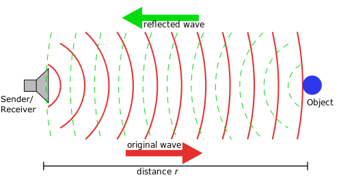
At the most basic level, a radar system works by transmitting a high-frequency radio signal in a certain direction, and detecting and processing reflections of this signal to determine whether an object exists in that direction.
Generally, the most important consideration for radar design is the amount of power received from these reflections at the receiving antenna. The received power can be calculated from the radar equation.
The radar equation shows that the received power is directly proportional to the transmitted power, the gain of the antennas squared, the wavelength of the transmitted signal squared and the scattering coefficient sigma of the target object. The received power is inversely proportional to the distance from the radar to the target object raised to the fourth power.
Of these parameters, we are only concerned with transmitted power P and range R. The radar is designed to output an effective radiated power (ERP) of 1 W, and has an upper limit in frequency of 2.4835 GHz, which corresponds to a wavelength of 12 cm. Since the antenna gain G and wavelength lambda will not change, in order to get the most received power, it is necessary to transmit as close to the transmit power limit of 1 W as possible.
The Honours Project radar is a frequency modulated continuous wave (FMCW) radar, and has two modes of operation: Doppler mode and Range mode, which will be discussed in later sections.
Radar Performance
The performance of a radar system is characterised by its maximum range and range resolution. The maximum range is the maximum distance at which the radar can detect the presence of an object. The range resolution of a radar is the ability to differentiate between close targets. For example, a radar system with a resolution of 5 m would not be able to resolve two people standing side by side; they would appear as one object on the radar.
By rearranging the radar equation for range, it is possible to make an estimate for the maximum range of the Honours Project radar system. An optimistic estimate for the range is approximately 96 m. The range resolution is based on the frequency range, and for this project is approximately 1.8 m.
Doppler Mode
The Doppler effect is the name given to the phenomenon of a change in the frequency of a wave when the observer is moving relative to the source of the wave. Many people have observed this effect in their lives when a vehicle with a horn drives past; the horn appears to be of a higher pitch when the vehicle moves towards you, and of a lower pitch when it moves away. The velocity of the source can be related to the perceived frequency of the wave and the waves actual frequency.
The Doppler effect applies to all waves, including the radio waves transmitted by radar. With the Doppler effect, the velocity of an object can be detected by a radar system. This is easiest when using continuous wave (CW) transmission. When the sine wave transmitted by the radar reflects off of a moving object, the reflected wave will have a different frequency to the original transmitted wave.
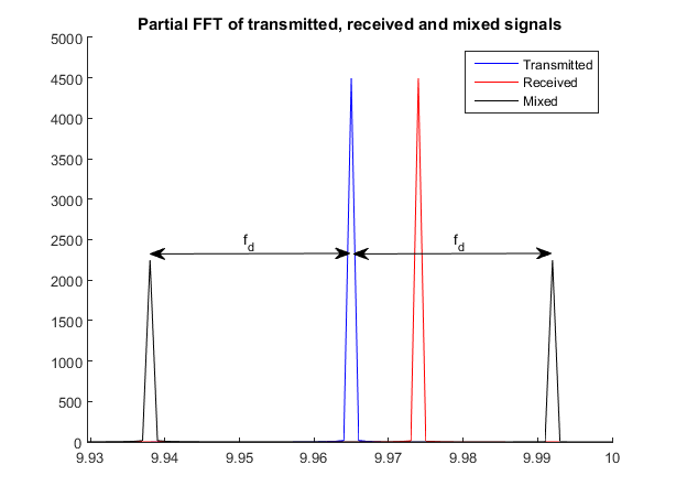
By mixing the transmitted and received waves, an intermediate frequency (IF) waveform is produced, which contains the sum and difference of the frequencies of the transmitted and received waves. The difference component of the IF signal will be at the Doppler frequency fd. This frequency value can be substituted for fd, along with the frequency of the transmitted signal f in order to find the velocity of the object v. A simplified simulation of the effect of mixing is shown below. In this example, the target object is moving away from the radar, as the frequency of the received signal is greater than the frequency of the transmitted signal.
The Doppler Mode of the radar has some limitations. Due to how the Doppler effect works, any stationary objects will not be detected by the radar, as well any objects moving tangentially to the radar. This is because only the component of the objects velocity that is radially towards or away from the radar can be detected. This also means that the velocity of an object not travelling directly towards or away from the radar will be less than the true velocity of the object, since only the radial component of the velocity is detected.
Range Mode
The range mode of the radar uses an FMCW signal to detect the distance of objects from the radar. It is not enough to use a CW signal; the signal must also be frequency modulated, resulting in what is called a chirp signal. A chirp signal is a signal for which the frequency changes with time. By using a time-varying voltage as the input to a voltage controlled oscillator (VCO) several different chirps can be used. Some common waves used for producing chirps are sawtooth, triangular, and square waves. For the Honours Project radar, the chosen modulation is a triangle wave, due to properties it has that make processing the received signal simpler.
When the radar transmits the chirp signal, it will receive a reflected, frequency shifted signal off of a detected object if one exists, and the transmitted and received signal will be mixed together as was the case for the Doppler Mode of the radar. However, the waveform in the Range Mode is more complicated, since the frequency is not constant, resulting in the IF signal shown here.
The image above shows that there is a high frequency component on the order of GHz, and a low frequency component on the order of kHz produced in the mixing process. The higher frequency component is not of use in the calculation of range, and can be easily removed in the signal processing stage, or with the application of a low pass filter after the mixer. After removing the high frequency component, all that is left is the low frequency component. In this low frequency component, the flat lines highlighted by rectangles in the image are what is used to calculate the range. Note that the image shows an idealised scenario of the range mode mixing, which differs from what would be seen in a real world case. However, the principles described here still apply.
The range of the object can be calculated using this frequency component, along with the bandwidth of the transmitted signal and the period of the wave used to generate the chirp.
PCB Design Considerations
A printed circuit board (PCB) is a compact board base designed to house a specific circuit. An advantage of using PCBs is that there is no need to worry about wires, since all connections between components are contained in the PCB itself in tracks of copper. Additionally, a circuit implemented on a PCB will often be much smaller than the same circuit implemented onto a breadboard. PCBs are used in almost every piece of modern electronics, from phones to computers to washing machines.
Many PCBs operate at DC or low frequencies, but in some applications, including radar, a PCB will be using high frequency signals. At low frequencies, the wavelength of the signal will be several metres in size; much larger than the size of the PCB, and so the voltage across the PCB can be considered to be constant. In high frequency applications however, the wavelength of the signal is comparable with the size of the PCB, meaning that the voltage can vary greatly across the PCB and cause it to function in unexpected ways. For example, the traces can operate like an antenna and interact with other parts of the circuit in unpredictable ways. To prevent behaviour like this, there are rules for designing PCBs at microwave frequencies (frequencies between 300 MHz and 300 GHz). Note that as the IF signal produced by the mixer is of a low frequency, on the order of kHz, these rules do not apply to the video amplifier segment of the PCB. The most important design considerations for the RF sections of the PCB are listed below:
- The circuit needs impedance matching at 50 ohms, in order to reduce losses and the voltage standing wave ratio (VSWR). The impedance of the traces on the PCB can be controlled by varying their width. This applies for any trace of greater length than the critical length, which is approximately 4.3 mm for this project.
- It is important to have a ground plane in the PCB for easy connections to ground using vias, which helps to keep traces short. Additionally, filling unused space in the component plane with copper, and connecting this fill to the ground plane with vias will help prevent interference.
- Via-hole connections to the ground plane should be placed approximately 1/10th to 1/20th of the wavelength of the signal apart, connecting the top plane to the ground plane in order to reduce coupling and interference from nearby sources.
- Parallel traces should be avoided when possible, in order to prevent coupling.
- No trace should make a 90 degree turn. This is in order to minimise reflections. Examples of good and bad turns in PCB traces are displayed in the image below.
There are also guidelines to follow for the power supply traces in the PCB. These considerations are also very important, and can potentially cause problems if neglected.
- If possible the power traces should be routed on a separate layer to the component traces.
- Power traces should be as large as possible in order to be able to carry the required current to components.
- For sensitive RF components where noise is a large concern (for example the LNA) power decoupling should be performed in order to reduce noise coupling into the component.
Results
Final Design
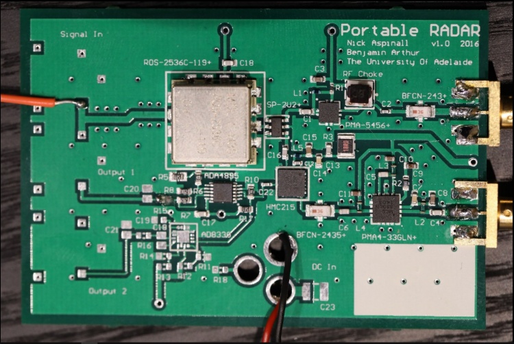
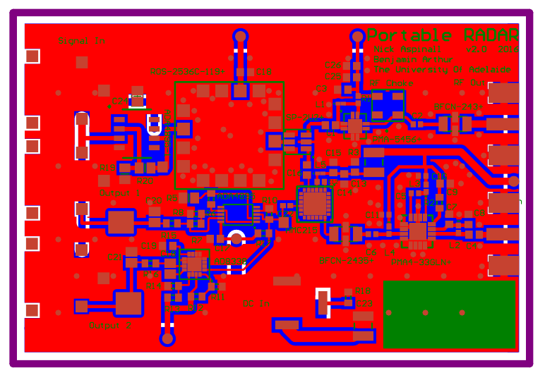
The PCB was manufactured using Entech electronics, using FR4 board material with a thickness of 1.6 mm and a dielectric constant of epsilon = 4.2 . Due to cost constraints a stencil cut out could not be purchased and the board was soldered by hand in house.
Transmit System Results
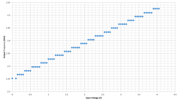
The first testing began on the transmitting system, applying a voltage to the VCO and measuring the frequency and frequency output of the system by connecting the output directly to a spectrum analyser. The cables used for measurements were found to have significant losses, and losses were measured using the RF signal generator at each power and frequency measured from the transmit system.
The transmitting system consists of the power amplifier and bandpass filter. From pre-calculations, the expected transmit power is 14 dBm
For the bandwidth of 2.4GHz to 2.5GHz, as required for this system, a minimum voltage of 2.1331V and a maximum voltage of 3.5803. Hence the transmission signal is a 50% duty cycle sawtooth wave, with a DC offset of 2.1331V, an amplitude of 2.8944V and a PRF of 200Hz.
The transmission power was smaller than expected theoretically, comparing to the data sheets, with measurements of 3dB lower power levels than expected.
The variations in power with frequency would be a result of changes of impedance in the transmission due to changes in frequency.
The receive chain was not operational upon fabrication. Testing of the chain with an input frequency of 700MHz and power of -30dBm netting an output power of 5dBm as expected at the amplifier output. Upon visual inspection of the mixer the alignment was off, and attempts to fix this issue were not successful.
PCB Design 2.0
After the manufacture of the initial PCB design, errors in layout were corrected and is present in the final PCB.
The changes are relevant to the practical manufacture and bypassing. The DC power supply has been flipped into it's correct place, and the circular through holes have been replaced with rectangular plated through holes. The capacitor DC input bypassing capacitor has been moved to accommodate for the size of the DC power jack, and so has the capacitor discharge resistor. Thermal relief has been added to the SMA jacks, to assist with soldering. Two more bypassing capacitors have been placed at the transmit amplifier, to better assist with bypassing at that point, particularly noise present from leakage of the VCO. Implemented is an amplifier for the VCO input, decreasing the drive required on the input source.
Conclusion
This thesis outlines the steps taken to design a portable Radar system into a PCB based implementation. The objective characteristics were a range resolution smaller than 2 and a range of approximately 100m for a target with a radar cross section of 1m^2
Through the analysis of different radar architectures and waveforms a stretch processing system was decided upon.The designed system had a theoretical range resolution of 1.8m and a maximum range of 100m.
Although the system was deemed not operational at completion, the transmitter system was operational, tested and voltage waveforms designed for its use. The fabricated system had increased portability comparing to previous works outlined in.
Although the manufacture objectives of the project were not met, the design objectives were and further work and manufacture of PCB design 2.0 will result in an operational system with the referenced above characteristics.
References
[1] G . Charvat, J . Williams, A . Fenn, S . Kogon, J .Herd. RES.LL-003 Build a Small Radar System Capable of Sensing Range, Doppler, and Synthetic Aperture Radar Imaging, January IAP 2011. (Massachusetts Institute of Technology: MIT OpenCourseWare), http://ocw.mit.edu (Accessed 19 Apr, 2016). License: Creative Commons BY-NC-SA
[2] M . Richards, J . Scheer, William . Holm Principles of Modern Radar Vol. I: Basic Principles, 2nd ed., SciTech Publishing, 2015.
[3] B. Mahafza, A.Elsherbeni Matlab Simulations for Radar Systems Design, 1st ed., Chapman & Hall, 2004.
[4] M . Jankiraman Design of Multi-Frequency CW Radars, 1st ed., McGraw Hill, 2007.
[5] J . Toomay, P . Hannen Radar Principles for the Non-Specialist, 3rd ed., SciTech Publishing, 2004.
[6] C. Coleman, An Introduction to Radio Frequency Engineering, 1st ed., Cambridge University Press, 2004.
[7] D . Pozar, Microwave Engineering, 3rd ed., John Wiley & Sons, Inc, 2012.
[8] "Mini Circuits - Global Leader of RF and Microwave Components", Minicircuits.com, 2016. [Online]. Available: http://www.minicircuits.com/. [Accessed: 22- Apr- 2016].
[9] M. Skolnik Introduction to Radar Systems, 3rd ed., McGraw Hill, 2001.
[10] B. Wadell Transmisson Line Design Handbook, 1st ed., Artech House, 1991.
[11] "RF / Microwave PC Board Design and Layout", jlab.org, 2016. [Online]. Available: https://www.jlab.org/accel/eecad/pdf/050rfdesign.pdf. [Accessed: 22- Apr- 2016].
[12] "AD8338 Technical Data Sheet", www.analog.com, 2016. [Online]. Available: http://www.analog.com/media/en/technical-documentation/data-sheets/AD8338.pdf. [Accessed: 5- Jun- 2016]. http://www.analog.com/media/en/technical-documentation/data-sheets/AD8338.pdf
[13] "High Speed PCB Layout Techniques", http://www.ti.com/, 2016. [Online]. Available:http://www.ti.com/lit/ml/slyp173/slyp173.pdf
[14] "High-Speed DSP Systems Design", www.ti.com, 2005. [Online]. Available: http://www.ti.com/lit/ug/spru889/spru889.pdf
[15] "Wireless LANs in the 2.4 GHz band FAQ", www.acma.gov.au, 2016. [Online]. Available: http://www.acma.gov.au/Citizen/Internet/Internet-services/Wireless-local-area- networks/wireless-lans-in-the-24-ghz-band-faqs. 60
