Projects:2017s1-135 A Low Cost Impedance Analyser
Contents
Abstract
This project has commenced in order to develop a low cost impedance analyser that can be used to perform measurements in a laboratory environment. The project will be able to significantly cut costs by utilising instruments and software already available from the University. The impedance analyser will make use of the voltage divider principle, where the impedance of a device under test (DUT) can be found by using the voltage divider equation. A signal generator will feed a signal into the main circuit and a digital oscilloscope will measure the resultant voltage output of the DUT. A resistor is placed in series with the DUT, where impedance matching will allow for higher accuracy results. Thus, a control mechanism circuit will also be developed to complement the main circuit.
The control mechanism circuit is comprised of a network of parallel resistors, where there are switches in each branch. The values of these resistors are per decade, from a minimum of 0.1 up to a maximum of 1 M. An FPGA will be able to determine which of the resistors has the closest value to the magnitude of the DUT’s impedance. The FPGA will then cause the switch to be closed, whilst leaving all other switches open. As a result, that resistor will then be in series with the DUT, completing the voltage divider circuit. This control mechanism is essentially behaving as an impedance matching circuit. A LabView program running on a PC will be developed that will communicate and control the developed impedance analyser. The signal generator, oscilloscope and impedance analyser will be connected to the PC via the USB protocol.
Preliminary results show that the analyser is able to acquire measurement data and hence it should be able to find the impedance of the DUT. The analyser should also able to find the transfer function characteristics of a filter. The obtained values will be compared against known impedances that have been calibrated with the analyser. The impedance analyser should be able to accurately determine the value of the known DUT, with a 0.1% accuracy tolerance.
Background
The fundamental working of the impedance analyser is that it will incorporate the voltage divider principle. A signal generator (controlled by a PC via USB port) will send a signal through the circuit. There will be a voltage drop across a known impedance that will be in series to the DUT (the value of the known impedance is determined from one of the known resistors in the small impedance network). The figure below shows the circuit configuration for measuring impedances.
The most suitable value (the resistor with the impedance closest to the load/DUT value) is selected by one of the relay switches (controlled by the FPGA by toggling the switch on or off). An oscilloscope will measure the voltage drop across the known impedance that has been selected. Thus, the impedance of the DUT can be found using the equation:
Vout = (Vin - Vout) * Zknown / (Zknown + Zdut)
Where:
Vout, is the voltage across the DUT
Vin, is the voltage from the signal generator
Zknown, is the impedance across the known impedance selected by the relay
Zdut, is the impedance across the device under test (DUT)
FPGA
The FPGA was programmed to be able to receive a serial signal and correspondingly relay a signal to the correct out put pin. The pin then allows the switching mechanism to create a series connection with the DUT. The below table illustrates the FPGA programmed output pins for the low cost impedance analyser switches.
LabVIEW
LabVIEW software is utilised to automate the hardware (AFG, oscilloscope and FPGA) functions of the low cost impedance analyser with a simple graphical user interface. The software stores results of the DUT measured by the low cost impedance analyser for further analysis. This section describes in-detail the developed LabVIEW software. To interface the hardware of the low cost impedance analyser with LabVIEW, instrument drivers are utilised. LabVIEW instrument drivers are a set of program-subroutines that create a communication link between LabVIEW and the connected instrument. In LabVIEW, predefined instrument drivers exist for both the arbitrary function generator and oscilloscope utilised in the design of the project. The Tektronix TDS 200 1000 2000 Series oscilloscope instrument driver is used to create a communication link between LabVIEW and the Tektronix TBS 1064 oscilloscope and the Tektronix AFG 1000 Series signal generator instrument driver is used to create a communication link between LabVIEW and the Tektronix AFG1062 arbitrary function generator [16] [17].
AFG Control Module The arbitrary function generator control module allows for the robust setting and injection of a signal into the low cost impedance analyser circuit.
Oscilloscope Control Module The oscilloscope control module allows for the systematic sampling and recording of voltage readings V1 and V2.
System-wide Control Automation
The below algorithm illustrates the skeleton of the algorithm of the system control under the user selecting the impedance analyser:
1. Calculate the frequency sweep array according to user input. 2. Send i^th frequency to the main loop, and define loop length (n) according to frequency sweep array size. 3. Set arbitrary function generator control module frequency and voltage according to user input; send error query chain to oscilloscope control module. Commence oscilloscope control module once error query chain received. 4. If first iteration: Perform oscilloscope setup prior to setting time base. 4b. Set time base according to frequency. 4c. send error query chain to signal processing module. 5. Commence signal processing module once error query chain received. 5a. Obtain impedance and signal if impedance needs to be recalculated with differently closed resistor. 5b. If appropriate resistor closed: Update all relevant GUI outputs; impedance and voltage data. Else loop through 3 – 5b. until correct resistor switched and impedance obtained; update GUI outputs on loop termination. Repeat 2-6, n times. Plot results against frequency.
Circuit Board Development
The circuit was initially realised on a prototyping veroboard in order to verify that the circuit setup is correct and functional. Once the switching mechanism (consisting of a BJT and relay combination) and the voltage divider were observed to be functional, the circuit was to be realised on a prototype PCB.
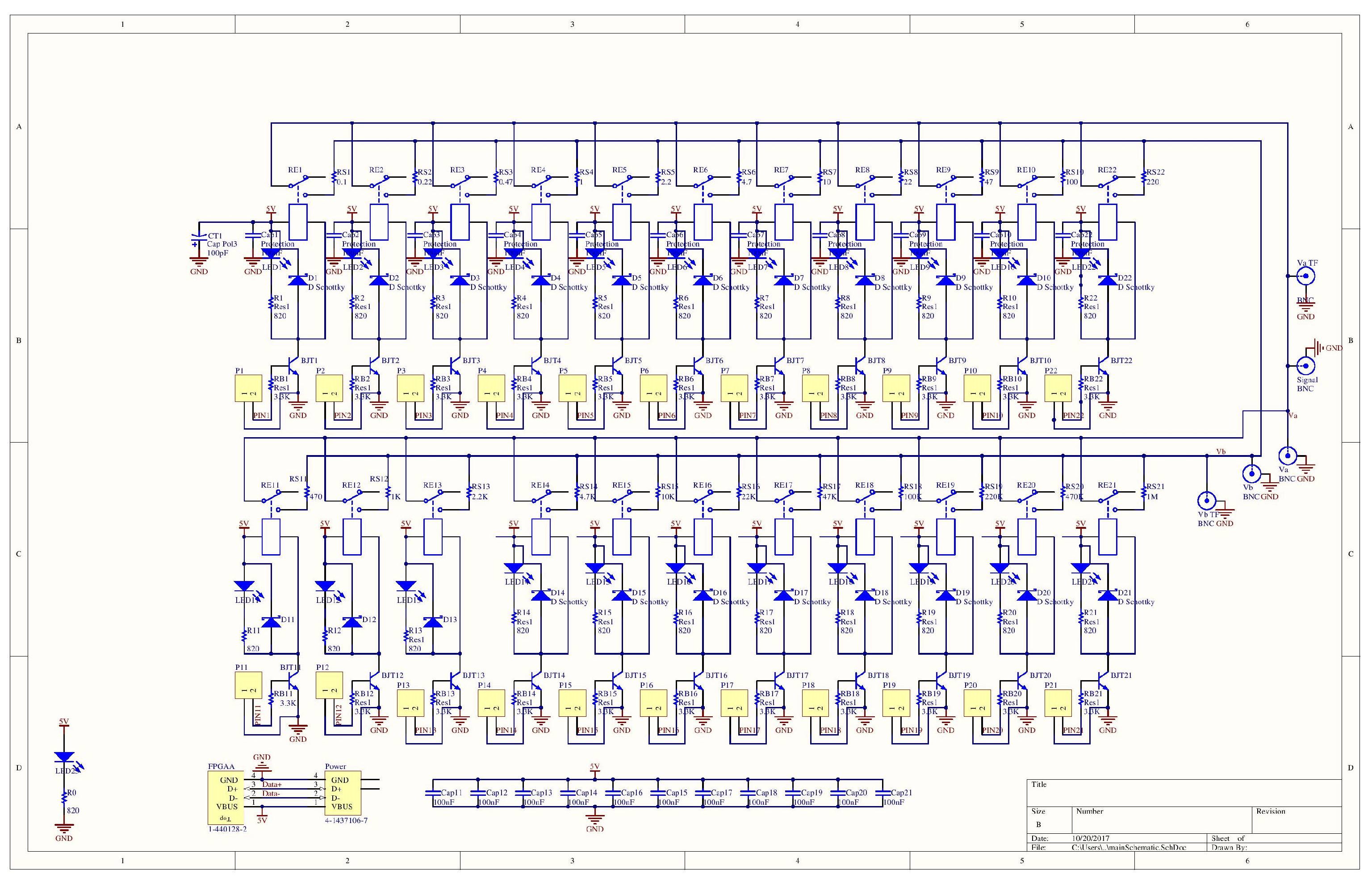
The PCB was developed using Altium, an eCAD software available from the University of Adelaide. The first step in the development of the PCB was to develop a full schematic of the circuit. This was an important stage as the schematic clearly outlines the entire circuit and shows the component arrangement. The developed circuit consist of many identical modules that are cascaded together in order to complete the switching mechanism. Once the entire circuit schematic was complete, it was realised into a PCB. This stage took quite a lot of time to complete as there is a large amount of components to be placed onto the PCB. Every component needed to be placed exactly in its intended position, which needed to be specified. This was also an important stage to determine the actual component models that will be utilised, as the component's footprint needed to be identified for the PCB design. Once the PCB design was complete, the design was exported into files that were then used for milling of the PCB.
TheSwitching Mechanism Schematic illustrates the final design of the switching mechanism for the low cost impedance analyser.
PCB Milling and Production
// Production and MIlling
// Don't forget to put lovely pictures!
Testing
Future Work
For an impedance analyser with a high degree of accuracy, open-circuit (OC) and short-circuit (SC) calibration techniques would need to be implemented in order to compensate for unwanted parasitic effects. The purpose of the open-circuit test would be to measure the effect on impedance caused by inductive components, whilst the short-circuit test would be intended to compensate for the capacitive components in the low cost impedance analyser. The principle of the OC and SC measurements can be illustrated by the model in Figure 27. The OC impedance of the low cost impedance analyser can be modelled as a parallel impedance to the uncompensated DUT impedance [14]. The SC impedance of the low cost impedance analyser can be modelled as a series element to the uncompensated DUT impedance [14].
The proposed process for calibration of the parasitic effects is described below:
1.Measure OC and SC impedances: Z_OC, Z_SC.
2. Measure uncompensated impedance of the DUT: Z_DUT.
3. Obtain admittance of DUT: Y_DUT=1/(Z_DUT..) and OC admittance Y_OC=1/(Z_OC..).
3a. Compensate for the effect of OC impedance on DUT impedance by subtracting the OC admittance: Y_A= Y_DUT - Y_OC
==> Z_A=1/Y_A
4. Compensate for the effect of SC impedance on impedance by subtracting the SC impedance: Z_DUTCalibrated= Z_A-Z_SC.
5. Output the compensated: Z_DUTCalibrated.
The figure above shows the model for the parasitic effects of the low cost impedance analyser.
Conclusions
The software and hardware integrated low cost impedance analyser device was found to be able to undertake the measurement of impedances and trasnfer functions by the end of the project. Accuracy of the device achieved was within 0.11% for a 1KOhm resistor for the final design. The promising results should however be considered with precaution, as calibration techniques still need to be applied to the system to ensure full accuracy is obtained.
Project Team
Student Members
- Muhamad Shahabuddin:
Bachelor of Engineering (Honours)(Electrical and Electronic) with Computer Science
- Filip Karisik:
Bachelor of Engineering (Honours)(Electrical and Electronic) with Finance
Academic Supervisors
- Professor Cornelis Jan "Keith" Kikkert
- Professor Cheng-Chew Lim