Projects:2018s2-279 High-Gain Antennas for Terahertz Communications
Contents
Abstract
According to Echolm’s law, data rate demands will exceed 100 Gbit/s by the year 2020 [1]. It would be impractical for the currently used Radio Microwave bands to support this data rate and so, an alternate solution will be required. A potential solution is progression to Terahertz band to utilize its higher available bandwidth available and hence, meet the data rate requirements. This project specifically investigates the requirements of antennas that will operate in the Terahertz band. Through analysis of existing high gain, high bandwidth antenna designs, this project aims to develop multiple antenna alternatives suitable for terahertz communications.
Introduction
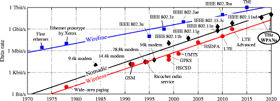
Edholm’s law, visually depicted on the red tread line in Figure 1.1, models the increase in data rates of wireless commutation standards over time. As can be observed, the model predicts that future standards will demand a data rate of 100 Gbit/s by the year 2020.
To meet this projected standard, communication technologies which utilize a greater frequency bandwidth and/or utilize this bandwidth more efficiently are required. This can be seen from Shannon’s Theorem (C=Blog_2 (1+S/N)) which shows that the data rate of a given channel, C is dependant on the bandwidth, B and signal to noise ratio, S/N of the given channel. The largest wireless band currently operating is at 60 GHz has a bandwidth of 7 GHz. To meet the 100 Gbit/s demand, this band would require a spectral efficiency of 14 bit/s/Hz, which is extremely challenging. An alternate solution, which can achieve the 100 Gbit/s demand with reasonable spectral efficiency targets, is the utilization of the terahertz band of frequencies located between 0.1 and 10 THz as shown in figure 1.2. This proposed solution is the focus area of this research project.
As observed in figure 1.2, the terahertz band in total has 9.9 Thz of bandwidth compared to 0.1 THz for the currently used Radio and Microwave bands, which results in a much higher potential data rates in the magnitude of Tbit/s [4]. As a result, the terahertz band can hold a steadier wireless data transfer rate than other high bandwidth frequency bands.
However, to take advantage of the terahertz band, there are a number of technical challenges, which must be overcome. For one, atmospheric and free space losses are increased in the Terahertz band, increasing the power loss that high gain antennas must overcome. Compounding on to this is the lossy Terahertz wave generation methods and amplified ohmic losses. Moreover, parasitic effects are amplified which increases the difficulty of impedance matching. Finally, dimensions tend to decrease with increasing frequency, which increases manufacturing difficulties. As a result, there are complications, which arise when designing terahertz band antennas that are not applicable to the currently used Radio and Microwave bands (see section 2 for more information). Resultantly, there is a shortage of antenna designs, which meet the criterion required for practical terahertz communications. Thus, further research into suitable terahertz antenna designs and how to overcome design challenges pertaining to terahertz antenna design is required.
Project team
Project students
- Nicholas Bonanni
- Stephen Li
Supervisors
- Dr Withawat Withayachumnankul
- Professor Christophe Fumeaux
Objectives
This project aims to accelerate the design and production of commercially available terahertz antennas. Also, the project aims to provide insight into how to overcome technical challenges associated with terahertz antenna design. To meet these ends, the objectives for this project will be to:
1) Evaluate range of high gain antenna designs for suitability for point-to-point communications in the terahertz band.
2) Scale, modify and simulate performance of a select choice of designs for operation in the terahertz band.
3) Manufacture chosen terahertz antenna designs and conduct practical tests to validate simulated results.
Background
Friis Equation
Friis equation is given as the following:
Where:
Pr=Recieved power at reciever antenna
Pt=Power transmitted by transmitter antenna
Gt=Gain of transmitter antenna
Gr=Gain of Reciever antenna
c=Speed of light in free space
R=Distance between reciever and transmitter antenna
f=Operating frequency
Although this equation does not take into the account attenuation losses in air, it does show the reason for the free space path loss (see the 1/f2 dependence of Pr). Additionally, it shows what factors can be altered to increase Pr and thus overcome the power loss induced by factors indicated in section 2.1. As can be observed, one could increase the power at the receiver antenna by reducing the f, but this would ultimately defeat the purpose of the project. Furthermore, there are limits to which Pt can be increased and R can be reduced in order to maintain practical power budgets and transmission distances respectively. Consequently, high gain transmitter and receiver antennas are required to overcome the power losses associated with Terahertz Band transmissions.
Antenna Gain
In antenna theory, the gain of an antenna is equal to the product of the antenna efficiency and directivity (G = e*D). The antenna efficiency, e, relates to the proportion of power inputted into an antenna which is radiated off as electromagnetic waves at the desired frequency. The directivity, D, relates to how much power is radiated in a singular direction compared to all other directions. As a result, high gain antennas radiate a large proportion of their inputted power in a singular direction [3].
S-Parameter
In the context of this project, the S parameter denotes the proportion of the power, which is reflected at the input port of an antenna in dB. It is reduced by increasing the matching between the antenna impedance and the impedance of its feed. As a result, it is beneficial for this parameter to be minimised.
Effective Area / Antenna Aperture
The effective area/ antenna aperture of an antenna is the area that receives power when acting as a receiver or transmits power when acting as a transmitter. Thus, as one can expect, the antenna aperture is directly proportional to antenna gain [3].
Phase Correction / Beam forming
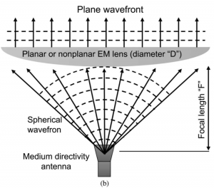
A method to increase the antenna aperture which is employed by many of the evaluated designs is phase correcting the output of a medium gain feed antenna. This process is illustrated in figure 2.1 below. As can be seen, the medium gain antenna produces a spherical radiation pattern, which propagates both normal and tangential to the intended direction of propagation direction. As a result, at a distance of “F” from the feed, the radiation pattern will be dispersed over a large aperture. However, there will be a large phase difference between the Electromagnetic (EM) waves across this aperture, which reduces directivity. To combat this issue, an EM lens or other type of phase correcting element is placed at “F” to direct the radiation in a singular direction to reduce the phase difference whilst maintaining the large aperture. Although many antenna designs employ this methodology, they all employ different types of phase correcting elements which will be compared in this report.
Literature Review
4.1 Metallic terahertz antennas
Metallic terahertz antennas are conventionally used for a relative high gain, a wide bandwidth performance and the low cost of commercial metal milling technology. These metallic antennas usually use metal as the surface, directly or effectively serve as a parabolic lens, to enhance the directivity of the radiation. However under terahertz frequency, metals can no longer consider as a perfect conductor. When frequency goes too high, the effective penetration area to the conductor will be reduced, hence the shallower area S will increase the resistance according to formula R=ρ* L/S Additionally, there is always non-zero capacitance between conductors, at higher frequency parasitic loss would become significant as well. As a result for these traditional metallic antennas ohm loss is no longer negligible. Although metallic antennas have a wideband performance and a high gain performance, generally over 20dBi, this type of antenna is still limited for the designability and non-negligible ohm loss.
Here two types of metallic terahertz antennas will be discussed:
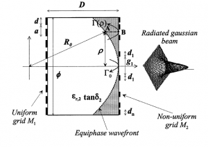
4.1.1 Non-uniform Mirrors Focusing Antennas[5]
The non-uniform mirrors antenna consists of two metal mirrors, one is a uniform grid mirror and the other is a non-uniform parabolic grid mirror.This metal parabolic lens would increase the directivity of the radiation. The lens surface changes the phase distribution of the electromagnetic (EM) wave to allow the plane wave to focus on its focal length. As shown in the radiated Gaussian beam in the figure, after the lens applied, the beam is focused on a spot. This non-uniform mirror focusing antenna is later feed by a rectangular microstrip antenna to validate the numerical result.
It shows that the antenna has a maximum gain of 17.6 dBi at 57.6GHz[5]. It agrees with the traditional metallic terahertz antennas that the gain performance is good and this particular antenna shows good compactness as well. Meanwhile a 3.9 dBi metal loss is also mentioned in this experiment. Still the ohm loss is a major consideration for metallic antennas.
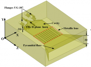
4.1.2 THz Metallic Lens Antenna[6]
THz metallic lens antenna provides a complete structure that consists of a horn that feeds the antenna, a metallic lens for phase compensation and a flare structure to further improve the gain performance.The metallic lens in this structure consists of ten metallic waveguide of same length, as shown above. The width of the waveguide is varied to achieve uniform phase distribution, under the condition that it only supports the dominate mode. The width is design to change the propagation constant of the dominate mode to compensate the phase delay.
The THz metallic lens antenna shows good gain and wideband performance. Beside the return loss is over 20dBi for this frequency band. The operating frequency is around 400GHz and the maximum gain is 27.6 dBi. Comparing to the convention horn antenna, which has a maximum gain of 22 dBi near this frequency band, the gain performance is increased by about 6 dBi.
4.2 Dielectric resonator antennas
As mentioned in the last section, metallic antennas are generally limited for the non-negligible ohm loss. To avoid such ohm loss at terahertz bandwidth, dielectric material used to replace metal. Dielectric resonator allows EM waves to bounce back and forth inside an area to form a standing wave. At a particular frequency the amplitude of the standing wave would be significantly large. Such resonator can increase the gain without suffering from ohm loss. However, this type of antenna will generally suffer from a narrow bandwidth, as the frequency bandwidth for resonance mode is very limited. Besides, this type of antenna also has strong optical anisotropy and a low gain performance due to substrate conduction loss.
Here two similar dielectric resonator antennas will be discussed:
4.2.1 On-chip higher-order-mode dielectric-resonator antenna[7]
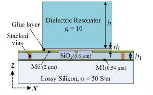
The on-chip higher-order-mode dielectric resonator consists of lossy silicon substrate, a thin silicon dioxide (SiO2) using standard CMOS technology and the dielectric resonator which operates at higher order mode ( in this case TE13 and TE15 ).It is worth noticing that this structure use half-mode cavity-feeding structure, so that the size of the structure is significantly reduce (a half).
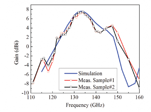
However, the main consideration of this antenna is still the gain and bandwidth. For TE13 mode the maximum gain is only 6.2 dBi at around 130GHz, and for TE15 mode the maximum gain is 7.5 dBi at around 135GHz. From the figure the gain decreases 3dB at around 125GHz and 135GHz, so the bandwidth is around 10GHz and it is very limited. Besides the maximum gain, 6.2 dBi is also limited.
4.2.2 On-Chip 3-D dielectric-resonator Antenna[8]
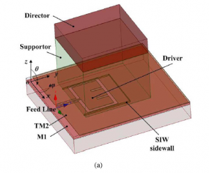
The on-chip 3-D dielectric resonator antenna is similar to the antenna mentioned above. The structure is same except there an additional support layer between the resonator and SiO2.For this structure, the design principle follows the general design rules for Yagi antenna by replacing three fundamental elements, driver dipole, reflector and a director in Yagi antenna. The driver and director can be replaced by patches and slots, while it is not recommended to add reflector since the substrate has low resistance. The supporter layer is designed to provide the sufficient distance and impedance matching between SiO2 and the resonator. While the bandwidth of this antenna seems good, the gain performance is still a problem. The maximum gain is 10 dBi operating at around 340GHz. The gain performance is still the major limitation for dielectric resonators.
4.3 Non-resonant antennas
The dielectric non-resonant antennas show good performance on the gain performance. They have wideband performance and will not suffer from ohm loss. Unfortunate some antennas require extremely complex design or fabrication process. Hence they are not suitable for design and manufacture by University devices for this project. Here two antennas are introduced.
4.3.1 All-dielectric rod antenna array[9]
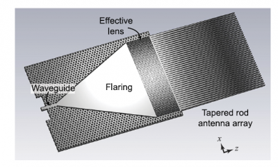
The all-dielectric rod antenna array consists of a flare section, a dielectric effective lens and several tapered rods.The effective lens is a silicon substrate consists of numerous air holes with different radius. The silicon wafer, together with air hole of different size will change the effective index of the unit cell hence compensate the phase delay in the silicon path. Effectively it serves as a lens to converge a spherical radiation EM wave to a plane wave.
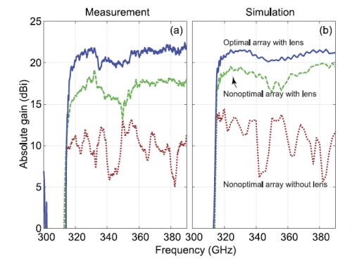
The gain-frequency plot shows a good gain measurement and a wideband performance. The maximum gain is around 22dBi and the -3dB bandwidth is at least 21%. However for this particular antenna, the design process is relative complex as for guided wave effective index is no longer suitable, modal index must be considered though it requires a more complex calculation. Moreover, the optimized case requires an 80*23 air hole array, which makes the fabrication much harder.
4.3.2 Corporate-Feed Slotted Waveguide Array Antenna[10]
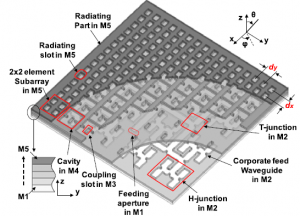
The corporate-feed slotted waveguide array antenna is a multi-layer waveguide structure that allows the EM wave to separate into different paths inside. For this particular design, it improves the gain performance by improving the etching accuracy. Instead using conventional diffusion process, the silicon wafer laminated plates are etched by deep reactive ion etcher process. They are plated with gold and then bonded with traditional diffusion process. By doing so it successfully increases the gain to 29.5 dBi at the operating frequency around 350GHz. Meanwhile it shows a wideband performance. However the fabricating process is becomes extremely complex and it is almost impossible to do by the University devices.
3-D Printed Phase Correction Method
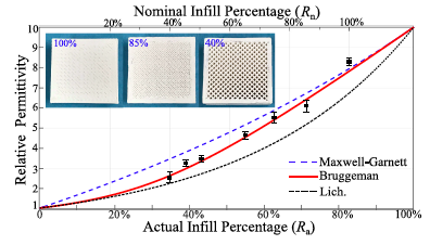
The chosen phase correction method for both of the project outputs is a 3-D printed PCS which varies the permittivity across its aperture in order to create a uniform phase distribution across said aperture. This is accomplished by varying the infill factor that the material is printed with at predetermined radial segments across its aperture. A visual illustration of the impact of varying the infill factor on a given material is shown in figure 5 along with a graphical representation of the relationship between infill factor and permittivity as determined by J. Huang et. al in [11]. This phase correction method was chosen as it greatly improves designability in comparison to the STHA as it can be modelled as a few concentric cylinders with varying permittivity as oppose to a dielectric slab with a large number of air holes. Likewise, the manufacturing process of this PCS is less well defined than the STHA. Therefore, although this may increase manufacturing complexity in the instance of this project, it will likely provide insight into the relevant manufacturing challenges which would improve future manufacturability of such designs.
Leaky Wave Design
Design Procedure
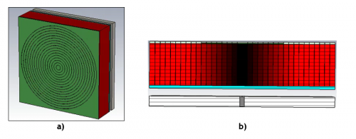
In order to save the costs and complexity of the design, the PRS, 3-D Printed PCS and material to air taper coupling were integrated into a singular block which is intended to be printed as one. The chosen 3-D printing material is PREPERM 3-D ABS DK 10.0 as developed by Premix Oy. By varying the infill factor as demonstrated in [25], a relative permittivity range of 2.0-8.3 can be obtained from 3-D printing with said material. Thus, the PRS, 3-D Printed PCS and Coupling material must have relative permittivity’s within this range. The intended configuration of the PRS, 3-D Printed PCS and Coupling is shown in figure 6.1 below.
PRS Design
Designing the PRS involves determining the aperture, cavity height and PRS thickness which produced the best performance as measured at the top of the PRS directly before the PCS. The required cavity height can be deduced using the physical properties of the ERA. The ERA acts as a high pass filter cutting off radiation with wavelength double that of the cavity height. As it was intended for the antenna to operate over the band of 220-330 GHz, the cavity height was chosen as 0.75 mm. The height could not be made lower as this produced large lobe spreading at higher frequencies due to the fast propagation of the TE1 mode in the cavity. Thus a cavity height of 0.75 provided an adequate trade off between the two. The required PRS aperture and thickness was then determined using computational optimisation using the CST [8] software. Through this procedure the optimum aperture was found to be 18 mm x 18 mm. Furthermore, the optimum PRS thickness was found to be 0.255 mm.
PCS Design
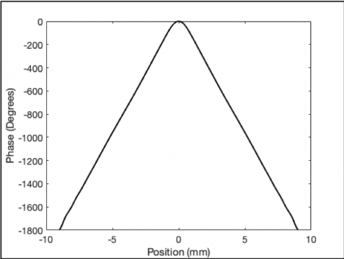
The 3-D Printed PCS is similar to the original PCS in the fact that a number of circular rings are placed across the PRS aperture for phase correction. However, now the permittivity of the rings is varied as oppose to the height to provide a varying phase delay across the aperture. As with the previously trialled phase correction methods, the phase across the PRS aperture was obtained via simulation in CST Design Studio[8]. The choice of phase correction frequency in this case was an iterative process. A range of frequencies from 180-275 GHz were trailed and optimum performance was found at 260 GHz. Thus 260 GHz was chosen as the phase correction frequency. The obtained phase for this design at 260 GHz is shown in figure 6.2 below:
As observed from figure 7.1, the phase across the PRS aperture varies approximately linearly with position. As a result, it was decided that the phase correcting segments would be of equal thickness. Moreover, it was found that 18 segments, 0.5 mm thick provided adequate performance without unnecessarily increasing the complexity of the structure. The phase of each segment was sampled at the centre of each segment as is tabled in table 6.1.
| Segment Identifier | Phase Measurement Position (mm) | Normalised Phase (Degrees) |
|---|---|---|
| R1 | 0.25 | -10.2 |
| R2 | 0.75 | -81.3 |
| R3 | 1.25 | -184 |
| R4 | 1.75 | -290 |
| R5 | 2.25 | -397 |
| R6 | 2.75 | -502 |
| R7 | 3.25 | -607 |
| R8 | 3.75 | -708 |
| R9 | 4.25 | -808 |
| R10 | 4.75 | -907 |
| R11 | 5.25 | -1010 |
| R12 | 5.75 | -1113 |
| R13 | 6.25 | -1218 |
| R14 | 6.75 | -1321 |
| R15 | 7.25 | -1426 |
| R16 | 7.75 | -1523 |
| R17 | 8.25 | -1629 |
| R18 | 8.75 | -1739 |
The required relative permittivity of each segment and the height of the structure can be found using similar methods as employed for the STHA above. However, in this case, a structure length must be chosen which yields the required phase correction range and the phase target must be chosen such that it centres the required permittivity range between 2.0 and 8.3. The phase delay given by a segment with permittivity, er and height, l is given by:
Thus, as the range of available permittivity values is 2.0-8.3, the phase correction bandwidth can be calculated like so:
Thus the required height of the 3-D printed PCS can be expressed as:
As can be observed from table 7.1, the phase correction bandwidth required is 1739. At the phase correction frequency of 260 GHz:
Thus, the required height can be calculated to be 3.8 mm . However to account for rounding errors and possible modifications that may have to be made during manufacturing, a length of 4.1 mm is used to ensure permittivity values remain in the required range.
The required phase delay which must be applied by each phase correcting segment for a given phase target can be found using:
ϕ = Phase Target+Normalised Phase
The required permittivity for each radial segment can be found using:
Determining the required phase target is an iterative process where multiple values are trialled until the used permittivity range lies within the manufacturable range. For this example, this occurred with a phase target of 3650 which yielded a minimum and maximum permittivity of 2.2 and 8.1 respectively. The required phase delay and permittivity for each segment is given in Table 6.2 along with each segments the inner and outer radius.
| Segment Identifier | Inner Radius (mm) | Outer Radius (mm) | Required Phase Delay (Degrees) | Required Relative Permittivity |
|---|---|---|---|---|
| R1 | 0 | 0.5 | 3639.8 | 8.1 |
| R2 | 0.5 | 1 | 3568.7 | 7.8 |
| R3 | 1.0 | 1.5 | 3466 | 7.4 |
| R4 | 1.5 | 2.0 | 3360 | 6.9 |
| R5 | 2.0 | 2.5 | 3253 | 6.5 |
| R6 | 2.5 | 3.0 | 3148 | 6.1 |
| R7 | 3.0 | 3.5 | 3043 | 5.7 |
| R8 | 3.5 | 4.0 | 2942 | 5.3 |
| R9 | 4.0 | 4.5 | 2842 | 4.9 |
| R10 | 4.5 | 5.0 | 2743 | 4.6 |
| R11 | 5.0 | 5.5 | 2640 | 4.3 |
| R12 | 5.5 | 6.0 | 2537 | 3.9 |
| R13 | 6.0 | 6.5 | 2432 | 3.6 |
| R14 | 6.5 | 7.0 | 2329 | 3.3 |
| R15 | 7.0 | 7.5 | 2224 | 3.0 |
| R16 | 7.5 | 8.0 | 2127 | 2.8 |
| R17 | 8.0 | 8.5 | 2021 | 2.5 |
| R18 | 8.5 | 9.0 | 1911 | 2.2 |
CST Macro Software was then employed to efficiently generate the structure in CST ready for simulating.
Taper Coupling Design
The 3-D printed PCS design is advantageous in terms of coupling design, as it allows the material to air coupling to vary in permittivity and hence be tailored for each phase correcting segment individually. However, the quarter wavelength design cannot be applied here as it would require relative permittivity’s below 2.0 which lies outside the manufacturable range. Resultantly, a taper coupling design was employed instead. The taper coupling design uses 1 or more dielectric slabs are placed in-between the material and air to reduce overall reflection losses in the transmission of RF power between the material and air.
As mentioned above, the taper coupling can be individually tailored to each individual coupling. However, it is important to ensure that the coupling does not vary too greatly as to compromise the phase correction process. Therefore, only two coupling configurations were used. Configuration 1, a combination of two dielectric slabs with relative permittivity’s of 5.0 and 2.0 respectively used for phase correction segments with permittivity greater than 5. The, Configuration 2, was a single slab of permittivity equal to 2.0 used for segments with permittivity less than 5. To reduce manufacturing complexity, both configurations were given equal lengths. Using this constraint and optimisation software included in CST[8], optimal performance was when the permittivity 5 component of configuration 1 was 0.0774 mm and the permittivity 2 component of configuration 1 was 0.109 mm. Resultantly, the length of configuration 1 was 0.186 mm.
Results
Physical Profile
The physical profile of the ERA with a 3-D Printed PCS and Taper Coupling is shown in figure 6.3 below. As can be seen from part b, the PRS, 3-D Printed PCS and Taper Coupling are integrated into 1 solid component. The PRS is indicated by light blue and lies above the first airgap. The 3-D Printed PCS is indicated by shades of red and lies on top of the PRS. Here darker shades of red indicate a higher permittivity. The coupling is indicated by dark (e_r=5) and light (e_r=2) shades of green and lies above the 3-D Printed PCS. Note that 3-D Printed PCS segments of higher permittivity require coupling configuration 1 (i.e. both dark and light green materials) whereas lower permittivity segments require coupling configuration 2 (only light green material).
Phase Correction
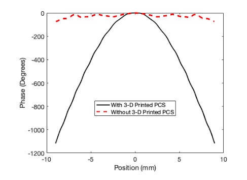
The phase plots for design with and without the 3-D Printed PCS are shown in figure 6.4 below. As can be observed, the addition of the 3-D Printed PCS reduces the maximum relative phase deviation from 1117° to 72.7°. Additionally, the nearly uniform phase region (i.e. region for which phase deviation is less than 50°) has increased from 3.20 mm to 16.5 mm yielding a 516% increase. This indicates that the 3-D Printed PCS performed effectively as the phase correcting component.
Radiation Pattern
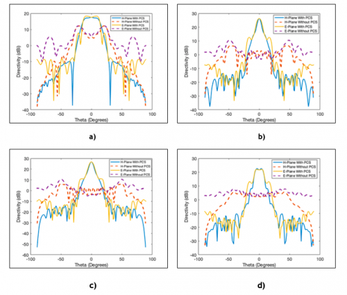
The radiation pattern of the ERA with 3-D Printed design is shown in figure 6.6 below at the low end of the spectrum (220 GHz), centre frequency (275 GHz), frequency of maximum gain (280 GHz) and high end of the spectrum (330 GHz). As observed, the 3-D Printed PCS greatly improves the prevalence of the main lobe across the entire 220-330 GHz spectrum. However, it can be seen from Figure 7.5 a) and d) that the effectiveness is reduced towards the ends of the spectrum. The -10 dB side lobe bandwidth is equal to 82 GHz (29.8%) and spans 226-308 GHz.
Broadband Performance
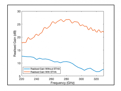
Figure 6.6 below shows the realised gain of the ERA with 3-D Printed PCS from 220-330 GHZ. As can be seen, the 3-D Printed PCS improves the gain of the ERA across the 220-330 GHz spectrum. The maximum gain of the design is 26.8 dB at 280 GHz which meets the lower bound of the gain requirement. The value of gain at the desired centre frequency is equal to 26.3 dB which also meets the lower bound of the gain requirement and deviates marginally from the maximum gain point. Additionally, the 3 dB drop off bandwidth is equal to 52 GHz or 18.9% (256-308 GHz).
S-Parameter Results
Figure 6.7 below shows the S-Parameter vs. frequency response for the input port (waveguide feed) of the ERA with 3-D Printed PCS. As can be observed, the 10 dB return loss bandwidth is inclusive of the range 220-328 GHz. Thus the 10 dB return loss bandwidth is equal to 108 GHz or 39.3%.
Conclusion
The above results provide sufficient evidence to suggest that the 3-D Printed PCS Design provides better performance than previously trialled designs. The design has provided the largest reduction in phase difference and the largest increase in the uniform phase region. Furthermore, the design also provides a minimum of a 6.3 dB increase in realised gain when compared to previously trialled slot fed designs.
Additionally, as the 3 dB drop off bandwidth is contained entirely within the 10 dB return loss and -10dB side lobe bandwidths, the total bandwidth for this design is 18.9%. The 3-D printed PCS also provides advantageous in terms of manufacturability as it can be manufactured using readily available 3-D printing techniques. Furthermore, the advancements made in this project have significantly simplified the design process of this particular phase correction structure.
Thus, as the given design meets the key performance targets set at the beginning of the project, it can be said that the project has been successful.
References
[1] T. Kürner and S. Priebe, "Towards THz Communications - Status in Research, Standardization and Regulation", Journal of Infrared, Millimeter, and Terahertz Waves, vol. 35, no. 1, pp. 53-62, 2013.
[2] "Overview", TeraNets: Ultra-broadband Communication Networks in the Terahertz Band, 2018. [Online]. Available: https://bwn.ece.gatech.edu/projects/teranets/index.html. [Accessed: 05- Oct- 2018].
[3] C. Balanis, Antenna Theory: Analysis and Design, 4th ed. New Jersey, United States: John Wiley & Sons, Inc, 2016, pp. 88-89, 791-792.
[4] M. Afzal, K. Esselle and B. Zeb, "Dielectric Phase-Correcting Structures for Electromagnetic Band Gap Resonator Antennas", IEEE Transactions on Antennas and Propagation, vol. 63, no. 8, pp. 3390-3399, 2015.
[5] R. Sauleau, P. Coquet, T. Matsui, and J.P. Daniel, ” A New Concept of Focusing Antennas Using Plane-Parallel Fabry–Perot Cavities With Nonuniform Mirrors”, IEEE Transactions on Antennas and Propagation, vol. 51, no.11, pp. 3171-3175, 2003.
[6] Z. Hao, J. Wang, Q. Yuan and W. Hong, "Development of a Low-Cost THz Metallic Lens Antenna", IEEE Antenna and Wireless Propagation Letters, vol. 16, pp. 1751-1754, 2017.
[7] D. Hou,W. Hong,W.-L. Goh, J. Chen,Y.-Z. Xiong, S. Hu, and M. Madihian, “D-band on-chip higher-order-mode dielectric resonator antennas fed by half-mode cavity in CMOS technology,” IEEE Trans. Antennas Propag. Mag. 56, 80–89 (2014).
[8] X. Deng, Y. Li, C. Liu, W. Wu, and Y.-Z. Xiong, “340 GHz on-chip 3-D antenna with 10 dBi gain and 80% radiation efficiency,” IEEE Trans. Terahertz Sci. Technol. 5, 619–627 (2015).
[9] W. Withayachumnankul, R. Yamada, M. Fujita, and T. Nagatsuma “All-dielectric rod antenna array for terahertz communications” APL Photonics, vol. 3, issue. 5, 051707, 2018
[10] K. Tekkouk,, J. Hirokawa,, K. Oogimoto, T. Nagatsuma,, H. Seto, Y. Inoue, and M. Saito “Corporate-Feed Slotted Waveguide Array Antenna in the 350-GHz Band by Silicon Process” IEEE Transactions on Antennas and Propagation, vol. 65, no.1, pp. 217-225, 2017.
[11]J. Huang, S. Chen, Z. Xue, W. Withayachumnankul and C. Fumeaux, "Wideband Endfire 3-D-Printed Dielectric Antenna With Designable Permittivity", IEEE Antennas and Wireless Propagation Letters, vol. 17, no. 11, pp. 2085-2089, 2018. Available: 10.1109/lawp.2018.2857497
