Projects:2014S1-42 Current-Voltage Tracer Experiment
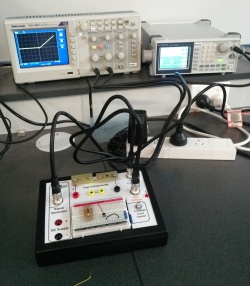
The aim of this project is to develop practical modules involving current-voltage characteristics for high school students and electrical engineering students in their first two years of study which illustrate basic electronics. Students will be initially introduced to simple circuit components including open circuits, short circuits, resistors and diodes then shown how different IV curves can be synthesised by series and parallel combinations of components. Further extension modules will include capacitors and inductors to demonstrate basic principles of filtering and resonance, transistors to demonstrate the importance of DC biasing and high power electronics to display current-voltage relationship of lightbulbs and DC motors.
This project will involve developing a number of prototype printed circuit boards with clear interfaces, instruction sets to suit different levels of audiences and report questions to reinforce the theory.
Contents
Team
Group members
- Kiyoon Kim
- Ben Agnew
- Luke Grinter
Supervisors
- Dr Wen Soong
- Dr Andrew Allison
Background
Current-voltage characteristics, or simply IV curves, describe the relationship between current and the voltage across an electronic component. It is a fundamental part of electronic circuit design as it allows us to model electronic components to achieve desired operation in various circuits. Some examples of such design include getting solar panels to operate at its maximum power point and getting transistors to operate in desired region of operations to achieve linear signal amplification in amplifier circuits.
Block diagram
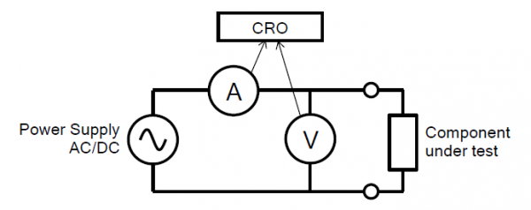
The following block diagram shows the basic set-up required to trace current-voltage characteristics on a Cathode Ray Oscilloscope.
The power source drives a voltage across the component under test to capture the current-voltage characteristics over a certain voltage range. The current measurement and voltage measurement blocks feed measured current and voltage data into the Cathode Ray Oscilloscope to display IV characteristics in real time.
Power Source
The power supplies available are:
- Signal generator - Variable frequency, 50ohm output impedance, max 10Vpk
- AC plug pack - fixed at 50Hz, fixed voltage, current up to about 1 to 2A
- DC power supply - DC only (requires memory in CRO), output adjustable up to 30V and 3A
The power required depends largely on what components we want to be able to test. We developed a list of components and then split them into two groups.
Low power components
These components typically draw less than 100mA and as such the signal generator is a suitable power supply.
- Resistors
- Capacitors
- Inductors
- Diodes (includes power, light emitting and zener diodes)
- Transistors (both BJT and FET)
High power components
These components draw a current in the range 0.5A to 3A and the lab DC power supplies were used.
- Light bulbs
- DC motors
- Fuses and Circuit breakers
Current Measurement
Resistor method
This works by passing the current through a resistor (of known value) and measuring the voltage drop across it. Since we can't directly measure the voltage (due the CRO probes been grounded) we designed a circuit that uses an op-amp to calculate the difference between the voltages on either side of the resistor (with respect to ground).
The resistor marked R is the current sense resistor and needs to have a value that is suitable for the amount of current that is to be measured. The other resistors set the gain of the op-amp. The value of R and the op-amp gain determine the volts per amp that the CRO sees.
Pros
- Simple and easy to understand and build
- Can be built to suit a large range of currents (by adjusting the value of R)
Cons
- Introduces a significant voltage drop (ie. the test components don't see the full supply voltage)
Hall Effect Sensor
The current can be measured by using a hall effect sensor to measure the magnetic field around the wire due to the current flowing in the wire. Due to the magnetic field been very week for small currents the current carrying wire is looped many times around a magnetic core to concentrate the field though the sensor in the gap. This setup can been seen in the following photo.
The sensor used was a UGN3503UA Hall Effect Sensor which requires a supply of +5V and has a quiescent output voltage of 2.5V which needs to be compensated for. With 15 turns of wire on the coil we found that it gave a volts per amp ratio of about 72mV/A
Pros
- Very robust - can't be damaged by applying to much current
- Small voltage drop across the current path - small impact on rest of circuit
Cons
- 2.5V offset needs to be accounted for
- More complex to build
- Only works for currents larger than about 0.5A
Transistor gate/base control
In order to test the IV characteristics between the drain-source (collector-emitter for BJTs) pins of the transistor we need to supply a gate (or base) voltage to turn the transistor on. We designed two different methods to do this.
Potentiometer voltage divider
Using the circuit shown below and by varying the potentiometer any voltage between 0.5V and 3V can be supplied to the gate terminal of the transistor. The 3.9k ohm resistor converts the voltage to a base current for the BJTs.
By adjusting the potentiometer students can see the curve move up and down on the CRO screen.
DC Step Function
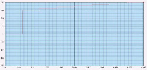
For the purpose of amplifier design, it is extremely useful to plot multiple drain current vs drain-source voltage characteristics of a FET for different values of gate-source voltage simultaneously. AFG Waveform software for the signal generator was used to achieve this by designing a DC step waveform that steps through different values of base voltages for each full cycle of sine wave from CH1.
The signal generator model available in Undergraduate Laboratory is GWInstek AFG-2225, which has the following specifications for arbitrary function generation:
- Sample rate up to 120 MSa/s
- 12 bit time resolution
- 10 bit voltage resolution
Assuming the frequency of CH1 sine wave is 1KHz, sampling the DC step waveform at 512 kSa/s with each step transition occurring every 512 steps results in a total of 8 different Id vs Vds curve for different values of Vgs.
The required voltage steps to give even spacing between curves over the range of the chosen IV curve scaling were determined experimentally by testing both BJT and the FET to be used in the practical (BC548 and VN10KM respectively).
Feeding the above waveform to the gate-source of the transistor from CH2 of the signal generator results in the following curve.
Complete Circuit
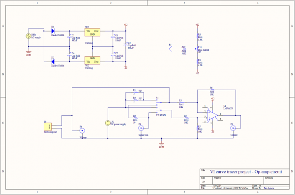
We chose to use the resistor current measurement method. Two different current sense resistors were included on the PCB - one for low power components and one for high power components. A DPDT switch was used to switch the op-amp circuit between each resistor. The op-amp power supply came from rectifying a 12V AC plug pack supply. The full circuit diagram can be seen in the following image. (click on image for a larger version)
Student Interface
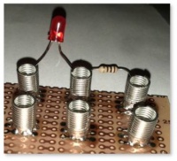
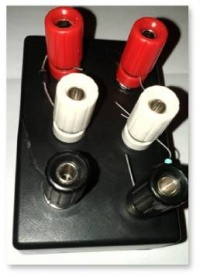
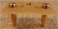
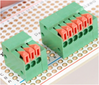
For the High School students it was decided that breadboard wasn't sufficient for the solder-less creation of the circuit. This was due to the complexity of breadboard as well as the limited time the students had (~45min session). Hence it was necessary to investigate some other solder-less options like springs, binding posts, banana plugs & sockets, wire wrapping and spring loaded terminal blocks.
 |
 |
 |
|
| Springs | Binding Posts | Banana Plugs | Spring Terminals |
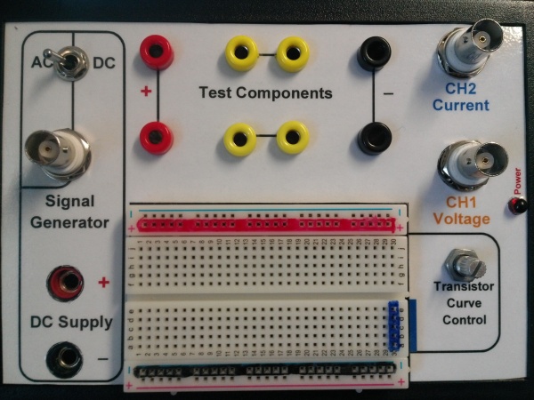
For the first box springs were selected in conjunction with an embedded small breadboard with this setup it would cover all applications. The springs would act as the "simpler" interface the High School student could use while the breadboard would allow for the more complicated circuits to be built eg. transistors, circuits with a large chain of components. After a review performed on the first box the team decided the springs were too flimsy, fiddly and difficult to solder wires from the PCB to itself. Following on from an idea developed on the first box using the breadboard as a medium small modules containing components were built as a plug and play idea. In their original form they were brittle and hard to use but changing to a better quality printed board and installing banana plugs such that they could be plugged into banana sockets allowed for a viable option. Leading on from this the second box stuck with the small breadboard, as this was useful, and replaced the springs with banana sockets so the plug and play modules could be utilised.
1st Prototype box
The first box and PCB built had the following components:
- Single PCB, 6.6 by 1.6 inches
- Op-amp gain of 1:1
- Low power resistor of 100 ohms 1/2W to give a volts per amp ratio of 100V/A
- High power resistor of 1 ohm 10W (as two 5W resistor in parallel) to give a volts per amp ratio of 1V/A
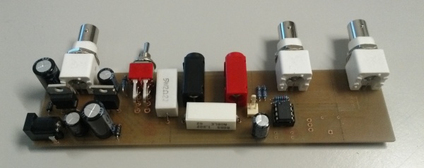
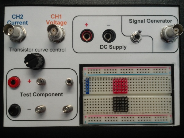
The following problems were found with this design:
- High power 10W resistor get quite hot with 3A flowing through it
- Volts per amp ratios don't match the ones available on the CRO
2nd Prototype box
The second box and PCB built had the following components:
- Two PCBs, 4.1 by 1.5 inches and 3.3 by 1.8 inches
- Op-amp gain of 1/2
- Low power resistor of 10 ohms 1/2W to give a volts per amp ratio of 5V/A
- High power resistor of 1 ohm 15W (as three 5W resistor in parallel) to give a volts per amp ratio of 500mV/A
- Added a 'power on' LED
Instructions and Exercises
High School Module
The targeted audience for this module is high school visitors for the School of Electrical and Electronic Engineering. This module is to be accompanied by a short presentation by the lab demonstrator as South Australian students lack electronics background due to the nature of the SACE curriculum. The target focus is to introduce high school students to basic building blocks in electronics - short-circuit, open-circuit, resistors and different types of diodes.
Resistors and Diodes
The targeted audience for this module is first year EEE students. The key learning objectives are introducing students to non-ideal nature of electronic components, understanding the behaviour different types of diodes and their applications.
Capacitors, Inductors, Filters and Resonances
The targeted audience for this module is first year EEE students. The key learning objective is to introduce students to current-voltage characteristics of capacitors and inductors to demonstrate basic filtering principles and the behaviour of simple resonant circuits.
BJTs and FETs
The targeted audience for this module is second year EEE students to serve as an introductory module to existing Level 2 Electronics Pre-Amplifier practical. The key learning objective is to support the theory covered in lectures to enhance student understanding of transistors and their behaviours in different region of operations. Students will be expected to carry out load line analysis and select appropriate DC bias points for a basic amplifier design.
Lightbulbs and DC Motors
The targeted audience for this module is first year EEE students. The key learning objective is to introduce students to current-voltage characteristics of Lightbulbs and DC motors. Students will initially experiment with the lightbulb to observe temperature dependent characteristics of high power electronic components and then use a Hand-Crank DC Motor to identify critical operating regions (No-load, stall and generation) of a DC motor.
