Projects:2014s2-72 Accurate Measurement and Modelling of a Switched-Mode Power Supply
In general, Switched-mode circuits are now the most common type of power supply in consumer appliances, including computers, and mobile telephones. However, models are not accurate representations of reality unless they are calibrated against actual physical devices.
The first aim of the project is to optimize the design for a switched-mode circuit, which must have an accurate theoretical model. The final aim of the project is to have an accurate state-variable based model of the converter that includes all the lossy parasitic aspects of the electronics components. Software such as Matlab and Proteus will be used to design switch-mode circuit simulation. The evaluation of the state-variable model will be executed and realized in Matlab. Software such as Altium should be used to implement the hardware circuit layout.
In summary, the extension of the project is building the state-variable model to reduce the lossy part of the circuit, thus, to optimize the circuit as much as possible, mathematical analysis terms can be needful in this aspect to improve the systematic methodology for the Low-loss switch-mode circuit.
Contents
Project Introduction
Exclusive summary
Nowadays, power electronics is providing the necessary interface between the electrical source and the electrical load. The electrical source and the electrical load can differ in frequency, voltage amplitudes and phases. The power electronics interface is used for transferring power from the source to the load by converting voltages and currents. It is believed that the use of DC-to-DC voltage conversion application is increasing among computers, TVs, electric cars and photovoltaic systems. Among them, the step down DC-DC converter a simple power electronic circuit to convert a DC voltage level to another lower DC voltage since switch mode power supply has the advantages of low cost, high efficiency, small size and weight. Thus, this project will focus on investigating the components and structure of switch mode conversion circuit then analyzing the performances by building the state-space variable model to optimize the circuit. Therefore, How does buck converter work? Look at Figure 1,S1 closes, current flows through the inductor and into the load, charging the inductor by increasing its magnetic field Vout reaches the desired value switch will be open continues to flow in the inductor the magnetic field collapses and the inductor discharges. Before the inductor completely discharge switch will be closed again. The cycle will be repeated.
Motivation
The motivation for this project is to study a switch mode energy conversion circuit, then in terms of the circuit analysis, It is worth to design and build a physical buck converter, thus seek several factors which may involve and affect the performances of the circuit such as power losses and circuit efficiency. Finally, try to improve the behavior of circuit by theoretical calculation and circuit simulation.
Objectives
Hardware section
Firstly, the aim is to design a physical switch-mode buck converter circuit that is provided by laboratory source and attached load, the circuit design tool such as Altium will be used to build the circuit. It is worth raising that before the PCB board manufacturing, the project team should design the circuit by theoretical calculation, then, design a simulation circuit in Proteus and run this high frequency circuit in Proteus to observe the current and voltage in each phases.
System modeling and simulation section
System modeling is the most important part in any system building and design work. The circuit model of this project depends on the performance of the simulation. The goal of the project is to predict the behavior of the switch-mode circuit before it is built. A very good system model provides designer with valuable information about the system optimization. Due to the difficulty in solving nonlinear equations, all the chips and parts will be put together in block diagram form and then simulated using MATLAB and Proteus. MATLAB and Proteus software will solve these nonlinear equations and also the software package can be used to simulate power converters. In continue by comparing the simulated mode, which is based on steady state matrix and real model will try to optimize the circuit.
Circuit optimization section
Finally, in order to close the gap between the state-variable model in MATLAB and physical circuit on PCB board, the project team needs to use both the model in MATLAB and Proteus to optimize the design for an improved physical circuit by testing and examining all the components. In addition, the theoretical analysis needs to be compared with the real circuit. The state-variable model will be compiled in MATLAB platform to calibrate the theoretical analysis by comparison with the actual data. The state-variable model will be used in observing and investigating the characteristic as well as the performances of the circuit. Consequently, from the state-variable model, project team should determine the parameters of components which may takes effect of energy loss, hence modify and improve the efficiency of the circuit.
Background
DC-DC buck converter circuits
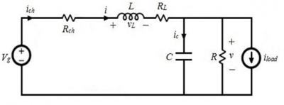
The buck converter is one of the simplest power electronic circuits to convert a DC voltage level to another lower DC voltage level. In Figure 2, the input voltage is generated an idealized DC source, The switch is usually a digital circuit which is called insulated-gate bipolar transistor (IGBT), IGBT opens when the control signal is 0 and closes when the control signal is 1.
In switch-on mode, the current flows directly through the load, because the diode is on reverse mode, while the circuit is open that means the switch mode is off, the current keeps flowing through the load and diode by the inductor. In Figure 2, theoretically, the purpose of the converter is to quickly open and close the switch, making the current flow through the inductor to the load represented by a resistor. If this state of quickly changing-over is in a high frequency, the current to the load will not decay, thus, making it fairly constant, producing a dc voltage in the output of the buck converter. Particularly, if the current of the inductor does not drop to zero during the conduction mode of the diode, then the circuit is being operated in continuous conduction mode. Otherwise, the circuit is in discontinuous conduction mode.
Simple Buck converter at on-state and off-state model
In steady-state, it is assumed that the input voltage, output voltage, output current and the duty cycle are kept constant and steady. Therefore, the current of the inductor flows during the entire switching time.
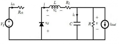
In continuous mode, there are two stages on the buck converter per cycle. In Figure 3, the first one is when the switch is on, the diode is on the reverse mode; In Figure 4 when the switch is off and the diode is conducting.
During the on-state model, the current of the inductor increases linearly with the time, due to the input voltage Vg and the voltage of the capacitor. By contrast, during off-state model, the current of the inductor decreases since the input current drops to zero, therefore, it is producing an opposite polarity voltage, which makes the current be able to flow through the diode.
System modeling
State-variable model at on-state condition
On-state with filter model When IGBT switch is at on-state, the Buck converter circuit is under on-state model which is shown in Figure 5. The voltage source is supplying 25V voltage at the load at where both the capacitors and inductor will be stored energy by charging from DC generator.
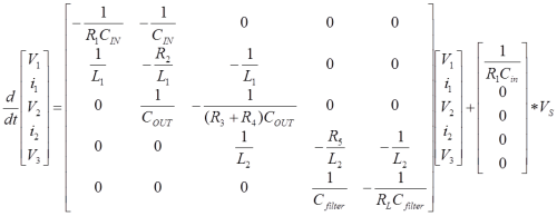
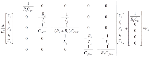
In Figure 5, we can apply Kirchhoff’s Current Law (KCL) twice of KCL1, KCL2 and KCL3. where the sum of the current flowing into the node is equal to the sum of current flowing out of the node. Furthermore, we can also apply KVL1 and KVL2 at where the sum of voltage around the loop is zero. With three KCL equations and two KVL equations, the following equation is expressed as vectors and matrices according to the form of 𝑥̇(𝑡)=𝐴𝑥(𝑡)+𝐵𝑢(𝑡)
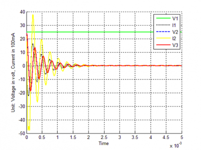
Finally, Figure 10 illustrates on-state simulation result.
State-variable model at off-state condition
By contrast, when the circuit is at off-state model, the voltage source would stop to charge the entire circuit due to the IGBT switch is off. Furthermore, the KVL1 loop will exist because the voltage source will still charging the input capacitor, meanwhile, there are storing energy in the inductor and output capacitor which result in loop KVL2 because the output capacitor and inductor will constantly dissipate the energy towards the load before the duty-cycle of switch on. Figure 7 shows the circuit of State-variable off-state model. Similarly, we can apply Kirchhoff’s Voltage Law KVL1, KVL2 and KVL3 at where the sum of voltage around the loop is zero, and also apply Kirchhoff’s Current Law (KCL) twice of KCL1 and KCL2, where the sum of the current flowing into the node is equal to the sum of current flowing out of the node.
Similarly, in Figure 9, with two KCL equations and three KVL equations, the following equation is expressed as vectors and matrices according to the form of 𝑥̇(𝑡)=𝐴𝑥(𝑡)+𝐵𝑢(𝑡)
Consequently, Figure 10 illustrates state-variable model off-state simulation result.
Time average model
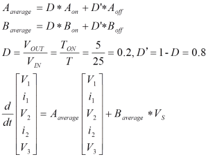
In the same way, we continue to utilize the following equations to calculate the output of Time-average model in Figure 11:
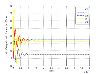
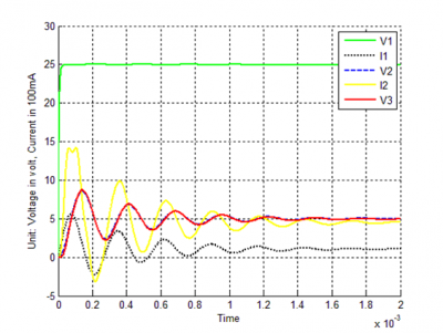
Consequently, the Time-average model simulation result in Figure 12 illustrates the overall result of input voltage, current I1, voltage V2, current I2 and output voltage. From Figure 12 we canobserve that the input voltage is at around 24.9V while the output voltage is at around 4.90V, by comparing with the simulation result without filter, we can perorate that the filter part has very little and slight influence on Buck-converter circuit.
PCB Realization in Altium
Selection of switch controller chip
According to the target of the project, which is a design an optimum buck converter, the switch has been replaced by IC. There are vast numbers of ICs that can be fit in this procedure, but the MC34063A has been selected because of following features.
• Operation from 3.0 V to 40 V Input
• Low Standby Current
• Current Limiting
• Output Switch Current to 1.5 A
• Output Voltage Adjustable
• Frequency Operation to 100 kHz
• Precision 2% Reference
• Pb-Free Packages are Available
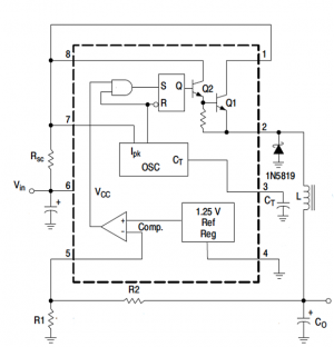
Figure 13 illustrates the inside structure of MC34063A and external components that can convert voltage to reduced level, in fact it is a general pre-design of the final circuit.
Circuit Simulation in Proteus
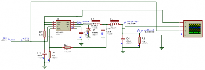
Creating a simulation of the circuit in one of the simulation software is one of the best ways to test the design. In this project MATLAB and Proteus has been used for this purpose. Realistically, the result that will be seen in the simulation will not be the same after manufacturing, because the couple of factors such as rout resistance, resistor tolerance and path thickness has not been concerned in the simulation, but the value of output will shows, is the project in the right track or not. To run the circuit by the button in Proteus, we can get the circuit simulation result in Proteus in Figure 14, which demonstrates the output result is also reasonable at 5.05V, thus we decide to design and manufacture the PCB as this circuit.
Altium Designer
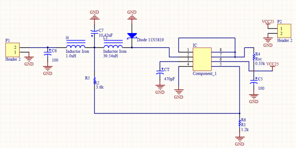
Therefore we make use of Altium Designer for designing and manufacturing the PCB. Altium Designer is one of the most convenient software in terms of design and creating PCB. Altium is able to make GERBER format of the design, which is the format of PCB creator machine. The first stage of design in this project was creating a schematic in Altium. Since the circuit includes an IC, the IC footprint must be designed firstly. Next stage was placing all other external components. The first step of this stage was finding the suitable component in real market and finds the exact one in Altium library, otherwise designer should design the footprint. Figure 15 shows the schematic of the circuit in Altium.
Bottom layer design of PCB
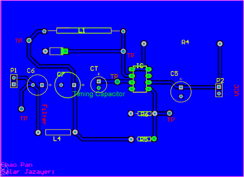
Figure 16 is Bottom layer design of PCB with polygon that omitted all left connections.
Final assembled PCB
Soldering is most important part in implementation stage. Any defect in soldering lead to damages to the board and improbable output. As the board is too small and all components are close together any mistake on soldering will lead to short circuiting the component and in some cases will damage the IC as well. Figure 17 is the Final assembled PCB.
Analysis of Output of PCB
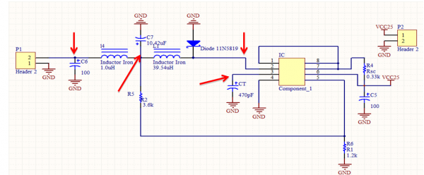
In terms of analyzing and testing the output of the circuit, not only the output has been checked but also the performance of all critical components has been monitored. In terms of increase the accuracy of the test, some test points have been added to the circuit, Figure 18 indicates the location of the test points in the board.
1. CT is timing capacitor and exactly will shows the switching time,Figure 19 shows the timing wave line is the normal timing wave for the switching.
2. Pin 2 There is another test point on the pin number 2 of the IC. Pin number 2 is output of a Darlington pair, switched emitter. As can be seen from the schematic the pin 2 will be connected to diode, Figure 20 illustrates this test point in the oscilloscope.
3. Diode, the test point number 2 in Figure 21 shows the diode behavior beside of the transistors effect.
4.Output-Filter This point is located in the output point, also it is connected to the capacitor c7, which is a output filter. Figure 22 shows the Output-Filter point in oscilloscope, The purple line is the output, as can be seen the output is stable and noise are really rare which is 4.87 instead of 5.00v and the reason is some transistor tolerance has been neglected.
5.Ripple and noise of the output, Figure 23 shows the calculation of the ripple and noise of the output, this graph has been created by using the cursor feature of the oscilloscope. Cursor has been set at two edge of the line and width has been calculated. The result shows 4.0mV fluctuation.
Optimized New PCB
In terms of addressing mentioned issues, team has been decided to manufacture another PCB, following is the list of
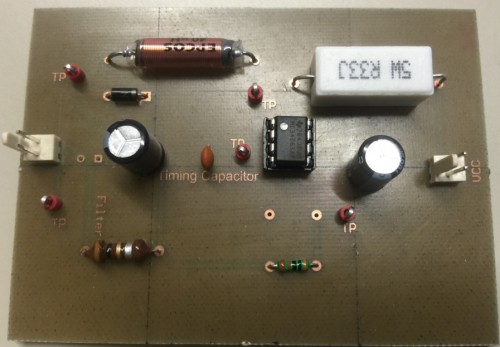
1.Adding a IC socket As the IC is one of fundamental component in this board and can be damaged for multi reasons the socket will provide a feature that IC be able to replace easily.
2.Adding test points Experience shows connecting probes to the components via bottom layer is not appropriate.
3.Bigger board Due to lack of space in previous board, it imposes some difficulties in measuring and other connectivity.
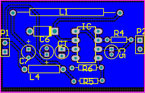
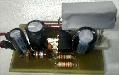
4.Future study Next students will analysis the new board easily. Figure 24 shows the bottom layer of the optimized new PCB and Figure 25 shows the assembled new PCB.
Conclusion and Future
Conclusion
In a word, during this project, firstly, we design the buck converter Switching Regulator Control Circuits based on the switching chip MC34064A, then, we build the ideal state variable model both in with filter condition without filter condition, then make comparison to find out the influence of filter towards the buck converter circuit. Afterwards, we simulate the buck converter circuit by making use of Proteus to simulate the high frequency circuit to observe the performance of test points and output of our design. We approved the design by observing the output of simulation and component has been purchased based on the simulation and previous calculation. Altium designer has been used for manufacturing the PCB, two board has been manufactured during this project which the second one is modified version of the first one. The target of the project as reaching to 5.00 volts, first board has been reached to 4.87 v and second board reduces this gap dramatically. The ripple range output voltage is 4.0 mv which is neglectable.
Future work
Regarding the state-variable model, the future work involves improving the model by trying progressive mathematical function to resolve the matrix in Matlab to optimize the state-variable model more accurately and analytically, also the comparing between ideal state variable and physical board must be observed further. Concerning the unexpected spark, our analysis showed by replacing the IC spark will be disappear. The new board contains a IC socket, so changing the IC due to the any damage will not be issue any more.
Reference
[1] Mohan, Ned, and Tore M. Undeland. Power electronics: converters, applications, and design. John Wiley & Sons, 2007.
[2] Cyril W.Lander, Power Electronics, Electrical engineering at De Montfort University, London,
[3] Michael Wong, Altium Designer Simple Schematic and PCB designing, University of Adelaide
[4] Jade Alberkrack, Theory and Applications of the MC34063 and uA78S40 Switching Regulator Control Circuits
[5] Richard C.Dorf, Robert H,Bishop, Modern Control system, Univeristy of Califoria, 2011
[6] Marcelo Gradella Villalva , Ernesto Ruppert Filho, BUCK CONVERTER WITH VARIABLE INPUT VOLTAGE FOR PHOTOVOLTAIC APPLICATIONS, Universidade Estadual de Campinas,2007.
[7] Vandana Jha* and Pankaj Rai, State Space Averaged Modeling of Basic Converter Topologies, VSRD International Journal of Electrical, Electronics & Comunication Engineering, Vol. 2(8), 2012, 566-575
[8] Alejandro Paz- Parra, Manuel Valencia, A State Variable Model for Considering the Power Inductor DC Resistance on the Open Loop Performance of a Buck- Boost DC to DC Converter, Journal of Multidisciplinary Engineering Science and Technology (JMEST) ISSN: 3159-0040 Vol. 1 Issue 3, October, 2014
[9] Robert W. Erickson, DC-DC Power Converters, Department of Electrical and Computer Engineering, University of Colorado, Boulder, CO 80309-0425
[10] Bengt Johansson, Improved Models for DC-DC Converters, Licentiate Thesis Department of Industrial Electrical Engineering and Automation, LUND UNIVERSITY,2003
[11] Rajvir Kaur, Navdeep Kaur, Mathematical Modelling of Buck Converter, International Journal on Recent and Innovation Trends in Computing and Communication ISSN: 2321-8169 Volume: 2 Issue: 5
[12] Intelligent Schematic Input System of Proteus, User Manual, Issue 6.0, Labcenter Electronics, November 2002
Group members
Salar Jazayeri
Pan Chao
Supervisor
Dr. Andrew Allison
