Projects:2015s1-71 Inductive Power Transfers
Contents
General Info
- Supervisor: Prof. Wen L Soong
- Advisor: Dr. Andrew Allison
- Students: Qian Zhao Yuqing Wang Xiaoqian Chen
introduction
Aims
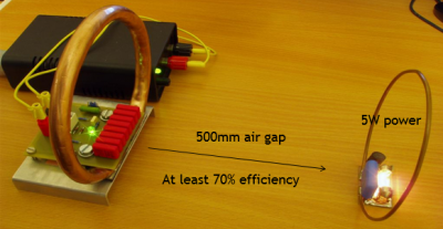
The aim of this project is achieving the inductive power transmission from a primary coil to a secondary coil, meeting at least 70% efficiency, through 500mm air gap and transferring 5W power to the receiver. Meanwhile, the size and weight of the inductive power transfer, which will be built, will also be minimized. In the end, the project aims to build an inductive power transfer which can successfully charges a mobile phone-sized device with above requirements.
Motivation
The project being undertaken is because as the technology has developed very sharply recent years, many new types of devices are produced which leading to the situation that everyone has many equipments need to be charged every day. However, firstly the bunch of wires and cables are easily tied with each other which is annoying and bothered, secondly, the exposure wires may have chance to hurt people. Finally, the wires and cables are easier affected by the extreme weathers. Therefore, this project has been focused on cause if it is successfully achieved, it would makes the differences that the working environment which full of devices will be beautified and people would not be bothered by finding no public charger in public place anymore. Then the safety of people who use them would be ensured. Finally, the wireless technology is more stable. In addition, according to the huge demand on the inductive power transfer technology, it is not only focused by engineers, but also concentrated by many commercial companies because it is also a commercialized technology which can makes many benefits, specifically, Oskar Rönnbäck(2013) [9] describes that during the next 10 years, according to the evaluations, the wireless power could be a billion dollar industry. Therefore, it will plays a critical role in the future electric market.
Significance
Oskar Rönnbäck(2013) [9] illustrates that there are benefits can be obtained from the wireless power system. The first is the environmental benefit. If the global medium-range-wireless standard is met, all the mobile devices can be charged by one wireless system which means many charger would be saved and also the numbers of using batteries would be reduced. Secondly, the social benefit is that the charge zones will be established in many publics which is convenient for people who carries many chargers every day.
Background
The inductive power transfer is a kind of wireless technology which is a electrical transmission from a power source to a receiving device without wires and cables between them. It is also belongs to the non-radiative technique which also called near-filed wireless power technology. Umenei, A. E. (June 2011) [14] illustrates that the energy of the primary coil stays at a short distance to the transmitter, when there is no secondary receiver arranged, the power would still around the transmitter rather than leaving it. Additionally, there are many applications we using in our daily life are under this technique such as electric toothbrush charger, electric vehicle charger, smartcard and so on. The wireless technology is one of the main advanced technology in the modern life, however it is an old technology. The inductive power transfer had been invented in 1800s when the transformer was developed (Oskar Rönnbäck 2013) [9].
Theories
Electromagnetic theory
There are some basic theories will be integrated and used to support the electromagnetic theory. According to [1], Ampere’s Law defines that the electric current passing through a closed wire loop will produce a corresponding magnetic field around the loop as the following figure 2 shows.
Faraday’s Law defines that the wire loop in the varying magnetic field will produce a voltage which called induced electromotive force (EMF) as shown by Sadiku [2], and Michael and Davidson [5]. According to [3] and [5], Lenz’s Law defines that the induced EMF, which was introduced in Faraday’s Law, will generate an induced current and hence induced magnetic field in the closed wire loop to suppress the change of the original magnetic flux. Electromagnetic theory is considerably important for wireless power transfer, because it can be applied to replace the solid wires. The following paragraph introduces it in detail. The figure 3 shows the electromagnetic field in a simple transformer, and the figure 4 is its detailed schematic diagram. Lincolncentral [4] shows in figure 4, the left part shows the primary winding which is injected with an AC current, and hence a variable magnetic field is generated around the winding. The secondary winding in this magnetic field will produce a varying induced EMF. Consequently, in the secondary winding an induced current will follow and create an induced magnetic field whose direction is oppose to the primary magnetic field as the right part shows. Additionally, the role of the induced magnetic field is to suppress the change of the primary magnetic flux and hence keep the magnetic flux constant.
Coupling
Coupling occurs when the change in current of one inductor induces a voltage in another inductor. According to the electromagnetic theory mentioned before and [5], coupling happens between the two windings of transformer, and the mutual inductance M can represent it as the following figure 5 shows. Among them, L_1 and L_2are the primary and secondary self-inductances, and coupling factor K is introduced to represent the relationship between self-inductances and the mutual inductance. The formula is K=|M|/√(L_1*L_2 ). Moreover, in order to simplify the transform circuit, the T model equipment circuit is used shown in the figure 6. The main profit of the T model equipment circuit is to convert the virtual electromagnetic field and coupling into an actual circuit diagram, which is benefit to analyze the transformer circuit.
Transform theory
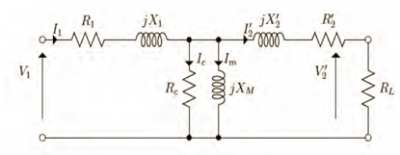
The wireless power transfer can be regarded as a special transformer, thus the basic transformer theory should be introduced. Govinda The following figure 7 shows the transformer equipment circuit. R_1 and R_2 are the primary and secondary winding resistances, and X_1,and X_2 are the primary and secondary leakage reactance. R_c is the core loss resistance and X_m is the magnetizing reactance. However, in order to remove the impact of the difference between the turns of primary winding N_1 and the turns of secondary winding N_2 , the secondary parameters can be referred to the primary terminal as the figure 8 represents. The formulas are here: a=N_1/N_2 , X_2^'=a^2 X_2,Z_2^'=a^2 Z_2,V_2^'=aV_2,I_2^'=I_2/a as shown by Govinda [6]. This full equipment circuit referred to primary is used for Mesh analysis in our experiment. For example, these formulas can be derived: Z_Total=Z_1+(1/(1/Z_M +1/(Z_2^' ))) I_1=V_1/Z_Total V_M=V_1-I_1 Z_1 I_2^'=V_M/(Z_2^'+R_L ) P_in=|V_1 ||I_1 | cos∅ P_out=〖(I_2^')〗^2 R_L η=P_out/P_in *100
Power amplifier
However, the power supplied by the signal generator cannot up to a value as high as 7.5W. The figure below shows the output power specifications of most RF signal generators.
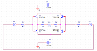
Different signal generator has different output level which commonly in the range from 10 to 100 mill watts [14]. While, the transformer can enhance the output voltage but it cannot improves the output power. As a result, for providing a suitable power for the transform circuit, a power amplifier is needed which can receives an electrical signal and amplifies and increases the power of the signal to meet the requirement and also provides the demanded frequency. In our project, the suitable amplifier would be the Class AB amplifier because it is a widely used type of power amplifier with less crossover distortion and higher efficiency. More specifically, the class AB push-pull output circuit is slightly less efficient than class B because it uses a small quiescent current flowing, to bias the transistors just above cut off [7]. In class AB each of the push-pull transistors is conducting for slightly more than the half cycle of conduction in class B, but much less than the full cycle of conduction of class A [7]. In another word, there are two devices in the circuit, each device operates the same way as in class B over half the waveform, so combining the two waveforms, the crossover distortion is minimized. Another advantage of the Class AB amplifier is that it is cheaper because using a complementary matched pair of transistors in emitter follower mode. The structure of the Class AB amplifier is shown below
Power amplifier design
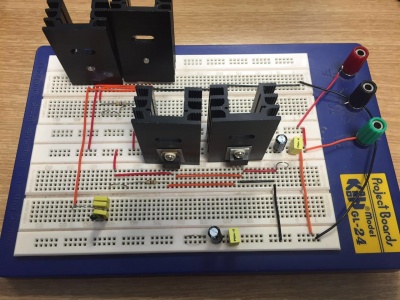
Class AB Power Amplifier design The power amplifier is built as the circuit
It can produce the output as below
Coupled coils design
The model of coils is shown
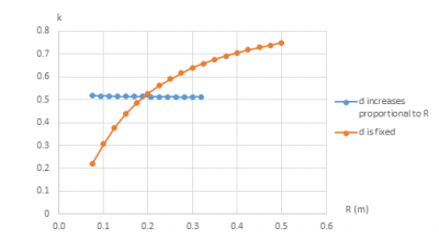
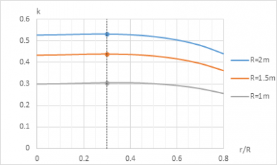
One for primary side and another for secondary, and two of them are exactly the same. The parameters of two coils include: the inner radius of both of them r, the outer radius R, the distance between two coils d, and the number of turns N. The main tool we used to simulate the parameters is called INCA, which represents Inductor Calculator. We can put the values we want into the software, and the result of self-inductance, mutual inductance, and coupling factor can be calculated. As we indicated before, the required distance between coils is 500mm, so firstly we want to investigate how distance influence the coupling factor.
Therefore, for obtaining a long distance performance, the outer radius should be designed large enough. When the inner radius is one third of the outer radius, the biggest coupling factor could be gained.
Power transfer circuit design
There are two alternatives about physical configuration of the design: coupled coils directly connecting to load resistance, or connecting load with additional resonant capacitor in each coil. The resonance is used to produce the same amplitude reactance with the inductance in each coil. Hence the inductive resonance and capacitive resonance can cancel each other out and only winging resistance lefts in order to increase the transferring efficiency. The equivalent circuit with resonances is shown in the following figure. Vin and Iin are the input voltage and current from electronic circuit, left side represents the primary coil, and right side represents the secondary coil connecting to the load resistance, and mutual inductance M combine them together. In each coil, there are winding resistance, inductance, and resonance.
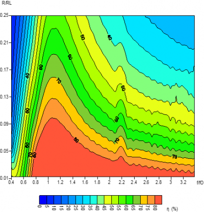
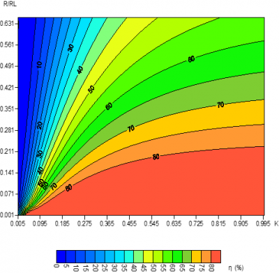
The major task is to explore how the ratio of actual frequency over resonance frequency, the ratio of winding resistance over load resistance, coupling factor affect the efficiency. Moreover, choosing winding resistance, inductance, coupling factor needs to trade off with the coupled coils design. Choosing input voltage, current, power also needs to trade off with the electronic circuit design. Additionally, choose proper resonance and load resistance in order to meet the objective of the project.
There are two efficiency contour graphs. Figure 1 shows that the change in efficiency when changing R/RL and f/f0 at the same time. Figure 2 shows that the change inefficiency when changing R/RL and k at the same time. We can get conclusions that when only increasing f/f0, the efficiency increases and then decreases. However, only increasing k or only decreasing R/RL, the efficiency increases. The other result is that the most effective factor to efficiency is R/RL, followed by k, and then f/( f_0 ).
Combination
As the result from the coupled coils design and the electric circuit design, the coils can be built.
Then, connect the circuit with the power amplifier, the load is connected with a bulb to demonstrate the result.
The light intensity of the bulb can vary as the distance of the two coils change. The result can be obtained as, when the distance is 500mm, input power is 8.5W, output power is 5.23W, the efficiency is around 61%.
Reference
Reference [1] Empowering Global Innovation, http://www.powersystemsdesign.com/idt-selected-to-develop-integrated-receiver-chip-for-qualcomms-wireless-power-technology
[1]. Fitzpatrick, R (2007, June 14). Ampère's Circuital Law [online]. Available: http://farside.ph.utexas.edu/teaching/316/lectures/node75.html
[2]. Sadiku, M. N. O, Elements of Electromagnetics, 4th Ed. New York/ Oxford: OU Press, 2007, pp. 386
[3]. Electromagnetics Explained, Elsevier Science Co., USA, 2002, pp. 75
[4]. Lincolncentral (2011), Electromagnetic Induction2 [online]. Available: http://www.a-levelphysicstutor.com/field-electro-mag-ind-2.php
[5]. Michael, W & Davidson (2003), Inductance [online], Available: http://micro.magnet.fsu.edu/electromag/electricity/inductance.html
[6]. Govinda, V (2013, November 30), Equivalent Circuit of Transformer referred to primary and Secondary [online], Available: http://kbreee.blogspot.com.au/2013/11/equivalent-circuit-of-transformer.html
[7]. Electronics projects (2013, February 2), Wireless Power Transfer, [online], Available: http://consultelectronicsproject.blogspot.com.au/2013/02/wireless-power-transfer.html
[8]. Carlos, M.” Mutual Inductance and Inductance Calculations by Maxwell’s Method,” 2014 [9]. O. Rönnbäck, Optimization of Wireless Power., Luleå: Luleå University of Technology, 2013,
[10]. M. Kiani & M. Ghovanloo, "The circuit theory behind coupled mode magnetic resonance based wireless power transmission," 2012.
[11]. T. Muhammad, S. Murtoza & Z.Anik, "Wireless Charger for Low Power Devices using Inductive Coupling," , 2012.
[12]. N. Madzharov & A. Tonchev, "INDUCTIVE HIGH POWER TRANSFER TECHNOLOGIES FOR ELECTRIC VEHICLES," J. Elect. Eng., vol. 65, no. 2, p. 125–128, 2014.
[13].C. L. W. Sonntag, E. A. Lomonova, J. L. Duarte., “Power Transfer Stabilization of the Three-Phase Contactless Energy Transfer Desktop by means of Coil Commutation,” Dutch Agency of Economic Affairs, 25 January 2008.
[14]. Umenei, A. E.. (2011). UNDERSTANDING Low frequency non-radiative power t. Senior Research Scientist.
