Projects:2017s1-111 OTHR Alternative Computing Architecture
Contents
Project Team
Daniel Lawson
Supervisors
Dr Braden Phillips
BAE Systems Australia (External)
Abstract
The aim of this project was to investigate the four computer architectures most commonly used for signal processing and radar to determine which would be most suitable for use in the JORN Phase 6 upgrade using auto code generation tools.
The architectures chosen were CPU, GPU, FPGA and ASIC with each compared across a range of metrics including run-time, utilisation, power, thermal and cost, base on previous work in computer architecture comparisons. Each system was explored for feasibility through experimentation on a wave propagation algorithm to evaluate device parameters and the measurement tools. Feasible architectures were then compared against each other using a second algorithm representative of expected workload where it was found that a GPU based system produced the best results with due to high performance with large data sets and strong developer support through tools and testing
As the project involved mapping a single algorithm to a number of different architectures, insight into the general process of high level synthesis was also discovered. It was found that even architectures designed for maximum portability required some manual rewriting of code to fully take advantage of parallelism with correct output.
Introduction
As part of the latest (Phase 6) upgrade to the Jindalee Operational Radar Network (JORN) project, BAE Systems Australia expect that the demand for radar simulation algorithms will increase over the duration of the networks lifetime. In expectation for this increased demand, this project will investigate the feasibility or a range of different architectures to identify the most suitable architecture for radar simulation. The methods found and results gained from this project will provide a basis for both strategic decisions for the JORN 6 upgrade, as well as a potential design guide for future algorithms.
Project Constrains and Assumptions
In was noted that JORN already possesses a large pre-existing code base designed for a CPU architecture. To reduce engineering costs of mapping the entire code base to a new architecture automatic code generation tools were used. This constraint acknowledges the fact that results may change if optimal implementations of each architecture were designed manually.
Methodology
1) An initial reference algorithm was mapped to each of the four architectures to show that it was possible to generate an implementation on that system with the tools available. 2) The system was then explored and the effect of different device parameters experimented on to determine optimal settings. 3) If the architecture was deemed feasible for use with JORN then the second algorithm that represents the expected system workload was mapped and data recorded for latency, utilisation, power, thermal and cost. 4) Each of these results was then compared against each other and plots produced. From these results and the observations made during implementation, the architecture that was most suitable for JORN was determined.
Reference Algorithm: Wave Simulation
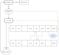
The initial reference algorithm was based on simulating a finite array for a specified number of time steps implementing the wave equations for a Gaussian Pulse source. This algorithm was chosen based on its simplicity with only a few operations on a large data set, the array size and number of simulations steps were both changeable and the application is somewhat related to radar.
Comparison Algorithm: Cooley-Tukey FFT
It was known that the JORN system uses a Polyphase channeliser to down convert the received signal, filter out noise and extract the relevant data from each channel in one system block. As this system was not implementable due to time constraints, a portion of the channeliser in the form of the FFT block was used. The Cooley-Tukey algorithm is a well known standard that computes an NxN complex Fourier Series with Nlog(N) time complexity rather than N^2 such as occurred in older implementations. Both a recursive implementation based on divide and conquer and an in-place bit shifting algorithm was generated with the recursive version preferred due to intuitiveness.
CPU Experimentation
Devices Available: Intel i5-3570k (Ivy Bridge) and Intel Xeon E5-2698 Tools Used: Compiler directives in the form of OpenACC through the PGI Compiler and OpenMP through the Intel Compiler.
Experiment 1: Choice of Compiler with No Directives used
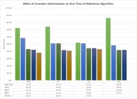
A number compilers were chosen and compared against the single core implementation of the reference algorithm where the following was found:
   1. With no optimisation the best performer was the PGI compiler while the worst was Intel.
   2. As optimisation levels increased this difference became saturated and minimal difference in run time was found.
Experiment 2: Effect of Compiler Directives
Using OpenACC compiler directives through the PGI compiler, a number of options for where to accelerate the code was tested with differentiating results as seen by the Table below:
Based on these results the following observations were made:
   1. Race conditions were discovered if trying to parallelism arrays over multiple simulations or at the output text file.
   2. Adding directives to small loops can decrease overall performance due to overhead in setting up memory.
   3. Large code blocks correctly parallelised can be sped up by a large amount.
Experiment 3: Effect of the number of Cores
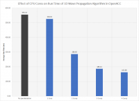
The final experiment conducted was to evaluate the number of cores. It was found that the compiler can be set to target any number of cores on the system, with difference latency results. As the number of cores were increased, up to a maximum of 4 the total latency decreased. However beyond this point the increased overhead started to dominate the program and thus performance decreased.
GPU Experimentation
Devices Available: NVIDIA GTX 1070 and NVIDIA Tesla K80 Tools Used: CUDA Toolkit Version 8.0. This provided access to the CUDA compiler and Visual Profiler to monitor all metrics.
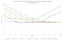
Experiment 1: Effect of Block Size on Run Time
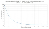
It was found that the GTX 1070 has a maximum block size of 1024 threads per block. As such an experiment was made to compare how the block size affects the run time. It was found that as the block size was increased, then more threads could be actively computed at once hence decreasing the overall latency. This relationship was not linear however as the use of more threads per block added additional overhead.
Experiment 2: Effect of Grid Size on Run Time
The second parameter that can be controlled in CUDA was the grid size. Each grid is made up of a number of blocks which are not able to communicate through shared memory. Thus using larger grids meant that initially the code performance was faster as block size increased, this speed up eventually reached a maximum value where further increases in block size caused decreased performance due to too much overhead. Using a constant relationship between grid and block size removed this decreases at the expense of worse initial performance.
FPGA Experimentation
Devices Available: Xilinx branded FPGA's Tools Used: Vivado High Level Synthesis (HLS), which is able to take a high level algorithm written in C++ and translate to a Verilog implementation on a target device.
Experiment 1: Developing a Correct Verilog Implementation of Algorithm
A test bench was first created using the initial single core implementation of the wave propagation algorithm. Then once a hardware block was implemented it was ran against the output of the test bench at both high level and as a Verilog design.
Experiment 2: Effect of Clock Target on Synthesis
Once it was shown that the design could be implemented, the next stage was to optimise the design. It was found that Vivado HLS would only optimise the design just enough to pass the clock constraint. Thus to get an optimal design this constraint would have to be reduced until it was no longer possible to reach the target. However decreasing the clock cycle could cause some blocks to take more than one cycle and hence the overall latency could increase. It was found that a clock target of 10ns produced the optimal results.
Experiment 3: Effect of Choice of FPGA on Results
The final area of experimentation for FPGA was to test which device was the best choice. As simulations were used, we had access to a large number of Xilinx devices, each with different costs and resources. Through running the design against each device, as per the table below the following was found:
   1. Even when using a small algorithm with less than 500 lines of code, synthesis targets were not met by all devices.
      The two cheapest available models, the series 7 Spartan and Artix both provided fewer `Digital Signal Processing blocks'
      than needed for synthesis.
   2. The Spartan 7 was the only device unable to reach the timing constraint of 10 ns.
   3. Each device produced a slightly different estimated clock despite having the same target constraint
   4. The most expensive device was not the fastest.
Based on a mixture of cost, utilisation and performance the Kintex7 was chosen as the preferred FPGA device.
ASIC Experimentation
Tools Used: As an ASIC is a fully custom device, Cadence Genus was used to take the Verilog output produced in the FPGA stage and produce a fully customised system.
Experiment 1: Effect of Timing Estimates
Once an initial implementation of the ASIC design was generated, the first experiment was to determine the best timing result. Similar to Vivado HLS, Genus performed lazy optimisation where it will only optimise enough to hit the clock targets. Thus the clock target was varied until an optimal value that meets the timing requirements were produced as seen in the Table below.
Based on this a number of observations were made:
   1. The optimal timing value was found to be 250ns to allow for 50ns of slack due to changes in the environment.
   2. As the clock setting was loosened, the total area increased, due to changing between large and small cell sizes based on the available library.
   3. Timing constraints did not affect the leakage power across the design.
   4. As timing constraint was loosened, the dynamic power decreased as large cell sizes were used.
Experiment 2: Effect of Power Constraints
The second constraint that could be modified in the design setup was the ratio of leakage to dynamic power. As the ratio was tightened such that less leakage power was allowed in the design, the overall power decreased. However at very tight bounds (1% leakage), the dynamic power was found to increase suggesting changes to the cells used in the design.
Feasibility of ASIC
While it was found that it was possible to generate a successful implementation of the design, due to the high cost of tools and the inability to accurately measure all metrics, it was concluded that an ASIC system was not feasible for use with JORN and hence was not included in the final design.
Comparison of Final Architectures
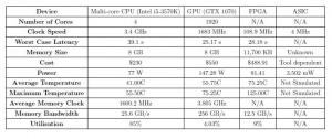
Through the initial experiments above, it was found that CPU, GPU and FPGA were feasible solutions to use in JORN, while ASIC was not due to high tool costs and not all metrics could be measured. The table below shows a summary of the implementation results of each architecture using the final Cooley-Tukey FFT algorithm.
Run Time
Latency was measured by running the algorithm on each architecture against a growing number of data points, increasing by a power of 2 from an initial 1024 points. In the FPGA case each data size was taken as a separate design and did not include I/O overhead. Both the GPU and CPU only timed the function call thus did not include set-up costs. It was found that the GPU performed slightly better than an FPGA at large data sizes, while both
single and multi-core devices performed far worse. At small data sizes (less than 1 million) it was seen that the single core CPU outperformed the GPU and FPGA due to lower overhead.
Utilisation
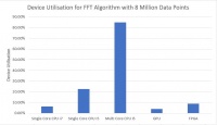
Utilisation was defined as the total percentage of the system an algorithm uses during run-time. In the software cases, this was measured during run time of the largest data size program through resource monitoring. In the case of GPU this did not include overhead such as memory transfers. For the case of the FPGA, the largest percentage of total resources (Look-up tables, RAM, etc.) for the largest data size was taken. It was found that the worst resource usage occurred with the multi-core CPU due to the compiler explicitly telling the Operating System to use all four cores whilst in all other cases the supervisor (OS or GPU scheduler) allocated the resources as needed. The lost utilisation was found to be the GPU suggesting most of the GPU was idle and a smaller device could be used.
Thermal Measurements
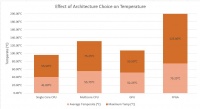
Temperature was recorded for each device through either the use of MSI Afterburner for the CPU or inbuilt temperature measurement systems. It was noted that the FPGA measurements have low overall confidence due to problems detecting the clock signal in Vivado while simulating the power report. It was found that the FPGA ran the hottest (if the results are considered valid), whilst the single core implementation ran the coolest on average, with the same maximum temperature as the GPU. It is noted however that the GPU fans do not even turn on until temperatures of 60 degrees Celsius are reached thus were considered to be within normal range.
Power Measurements
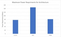
As gaining accurate power measurements of a single component of a larger computer system was not possible with the tools available, power measurements were based on manufacturer recommendations. The summary of power measurements show that the FPGA and CPU consume similar amounts of power whilst the GPU is considerably more power intensive leading to increased running costs.
Cost Considerations
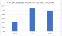
As each generation of architecture is constantly being updated and released, accurate cost measurements were hard to acquire with new models released across the duration of the project. When considering the relative differences in cost, the price of the GPU and FPGA were similar with CPU costing about half the price of the others. However it is likely that both the GPU and FPGA would act as a co-processor and thus still requires a CPU to run further increasing the cost of these architectures.
General Case Mapping Insights
During the implementation of both the wave propagation, reference algorithm and the final comparison FFT algorithm a number of observations were made regarding the general case of mapping a pre-existing high level algorithm to a range of architectures. Each of these points are discussed here.
Parallel Programming and Race Conditions
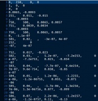
As found that parallellising an algorithm without first considering the effect it will have on any critical sections can lead to incorrect results. When using compiler directive to parallelise a file-write loop it was found that the algorithm would produce incorrect formatting into the text file such that the output was unreadable. Although the function to compute the arrays was performed correctly in a single thread, the output file was written in multiple threads which could run at the same time. Due to race conditions the order in which output text was written was not preserved or guaranteed to complete before the next thread tries to write leading to the jumbled order.
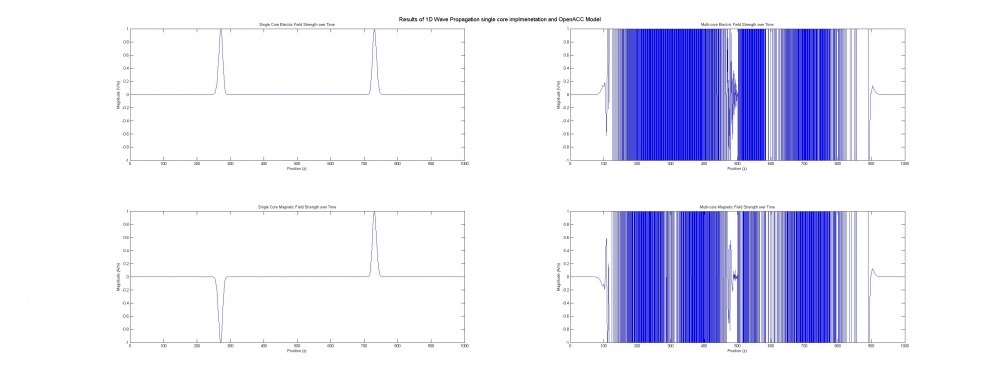
Additionally when parallelising multiple runs of the same program with each thread using the same memory locations for the array. Hence although each run through the program could occur in its own thread, all threads shared the same memory thus the array would be comprised of data from all four cores at any one time. The text file was written in the correct format as it occurred in after the threads converged, plots were produced that show the incorrect output.
Performance Overhead
It was noted that each architecture introduced some form of overhead that affected results:
   CPU: When accelerating one of the function loops it was found that performance decreased by a factor of 0.87.
        This occurred due to the amount of time spent in the parallel loop being less than the overhead introduced by
        copying data into the shared memory to perform parallel operations.
   GPU: It was seen in the previous section that small data sizes performed faster on the single core CPU than an accelerated GPU.
        This was due to the increased overhead introduced from the set-up required such as copying the code to and from the host
        and synchronisation dominating the time spent in the kernel.
  FPGA: As the FPGA would likely act as a co-processor, the biggest area of overhead concerned I/O. Thus delays in transferring
        data to and from the FPGA becomes significant. Additionally depending on the FPGA, common blocks such as multiplication
        and memory might exist in a `hard block' to improve speed-up. If no such block existed then overhead is introduced as
        the system would have to implement additional methods such as the exponential function.
  ASIC: Similarly to the FPGA, an ASIC would be used as a co-processor in a larger system. However as the system lacks
        reconfigurable blocks implementing basic operations, full freedom is allowed which could produce a more efficientdesign.
        The biggest overhead is instead felt at design time with massively increased synthesis time of more than 20 minutes
        compared to the seconds that CPU and GPU's took to compile or even the 5 minutes taken by the FPGA.
Recursion and Other Architectures
Recursion is an advanced computer science concept designed to simplify a problem through repeatedly calling a similar version of itself until a base case is reached. When trying to use recursion on non-stack based architectures such as GPU and FPGA without first implementing a stack caused problems to occur.
   GPU: Recursion on GPU is a relatively new idea, with new version of CUDA implementing both recursion and dynamic parallelism
        (allocation of memory during parallel code) through an extension to their programming model. It was not possible to
        implement the recursive version of the FFT algorithm due to the use of dynamic memory at each stage of the stack.
  FPGA: Vivado HLS relies on a subset of C functionally hence does not support recursion. This severely limited the scope
        of usable functions in the high level algorithm that will be translated into Verilog.
Thus in both cases, large manual rewrites of the algorithm were required through switching out the recursive implementation with the in-place bit-shift version.
Use of Language Techniques
Aside from the multi-core implementation, each of the architectures used resulted the translation of C++ code to a subset of C++ that could then be synthesised into a new language and architecture. This resulted in numerous technical challenges for each system:
   GPU: CUDA, which appears language to C++ but is a separate language was used on the GPU. The compiler (NVCC) was able to
        handle a mix of host and device code hence allowing standard C++ source code to be used on the host. However C++ methods
        were not usable on the GPU and instead equivalent methods were needed through the CUDA libraries such as CUDA Math and
        cuFFT38. Without support from NVIDIA or open source libraries, even heavier rewrites would be necessary to accelerate
        code onto a graphics card.
  FPGA: Vivado HLS uses a subset of C, C++ and System C that can be synthesised into RTL. Most of the system libraries were
        supported by Xilinx such as the Math and Complex number library such that minimal changes to the code were needed. The
        only change necessary was converting fixed width types such as int64_t with long longwhich was at least 64 bits.
  ASIC: Rather than directly using modified C++ code as with GPU and FPGA, Genus instead used HDL code (Verilog) as an input,
        which was supplied from the output of Vivado HLS. The only issues faced were in setting up the design scripts to
        correctly handle the output name style such as using ap_clk rather than clk.
Lessons Learnt
Tools and System
One of the major problems found during the project was acquiring a concise set of tools that were able to handle all aspects of the project. Due to restrictions on licensing some of the choices were limited and thus could not be changed, with others chosen based on research. Some tools such as the CUDA programs were run
on Windows to have access to the GPU, whilst others such as PGI were only runnable on Linux. This meant that a Virtual machine was needed to ensure the tools ran on the same CPU but likely affected the results. This restriction also limited the use of the supercomputers. Upgrading the supercomputer to utilise the latest tools and to record all metrics could have allowed for more varied results.
Control and Hardware
A large number of programs were used in the project across multiple systems. Over the duration of the project some of these systems underwent upgrades changing parts of the hardware such that the initial results using the reference equation may have slightly different specification than the final algorithm. This meant that the results were not as accurate as they otherwise could have been if a single machine was used that contained all CPU and GPU devices and was not modified over the duration of the project.
Focus on Scope
When the project first began, the scope specified the use of a single algorithm to compared the four architectures. However due to delays and the complexity
that would be introduced by such an algorithm, the scope of the project was changed to allow an initial investigatory algorithm. This reference equation focused on the tools and developed insight into the general case of mapping architectures. This came at the reduction of time spent on the final comparisons. Thus finding a balance between exploration and comparison would have lead to a more balanced project.
Future Work
Addition of New Architectures
The choice of architectures used in this project was limited by availability and thus we were not able to use the latest and best of each technology. In the duration of the project new architectures for both GPU and CPU were either announced or released. Thus a range of new architectures could be used in a future version of this project. These include:
   NVIDIA Volta: The newest architecture that NVIDIA intends to release in 2018 is the first GPU to make use of TensorCores. TensorCores are
                 NVIDIA's implementation of a processor designed for big data and machine learning applications including Google search and
                 translate to accelerate neural network computation.
   AMD Ryzen and Intel i9: AMD and Intel have both released their newest CPU architectures with ever increasing number of cores. These
                 both could be potential areas of look into.
   Other GPU Cards: both the use of AMD graphics cards, OpenCL and the Vulkan GPU architecture could all be areas of interest in GPU domain.
   Other Architectures: numerous architectures that were not considered could be investigated including non Xilinx FPGA devices, Raspberry
                 PI and even Mobile Graphics.
Role of Hardware
Budget restrictions played a major role in the scope of this project and as such simulation of hardware was preferred over testing on real devices such as fabricating an ASIC or programming an FPGA. Thus using the projects results, the most viable architectures could be expanded into a range of physical hardware options allowing factors that were not identified during simulations such as noise and the effect of the environment. This would give a better overview of each architectures strengths allowing for more accurate recommendations.
Full System Test
The other major limitation made on the projects scope was the algorithm used. Due to Defence security issues, we were not able to access the full JORN system and instead relied on approximations of a typical workload. The project could hence be expanded to produce results using the entire JORN system and compared against the chosen architecture using real world data. This would then allow a full comparison with the existing system to determine if the proposed architecture would improve performance.
High Level Synthesis
This project explored the issue of taking a pre-existing algorithm written in a high-level language such as C++ mapping it to a range of target architectures. Thus this project could be used as a base for an investigation into the general process of high level synthesis as it extends to the general case.
